MOSFET Basics - Electrical and Computer Engineering at UNC
advertisement
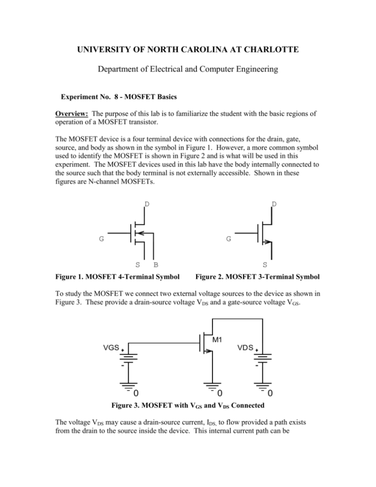
UNIVERSITY OF NORTH CAROLINA AT CHARLOTTE Department of Electrical and Computer Engineering Experiment No. 8 - MOSFET Basics Overview: The purpose of this lab is to familiarize the student with the basic regions of operation of a MOSFET transistor. The MOSFET device is a four terminal device with connections for the drain, gate, source, and body as shown in the symbol in Figure 1. However, a more common symbol used to identify the MOSFET is shown in Figure 2 and is what will be used in this experiment. The MOSFET devices used in this lab have the body internally connected to the source such that the body terminal is not externally accessible. Shown in these figures are N-channel MOSFETs. D D G G S B Figure 1. MOSFET 4-Terminal Symbol S Figure 2. MOSFET 3-Terminal Symbol To study the MOSFET we connect two external voltage sources to the device as shown in Figure 3. These provide a drain-source voltage VDS and a gate-source voltage VGS. M1 VGS VDS 0 0 0 Figure 3. MOSFET with VGS and VDS Connected The voltage VDS may cause a drain-source current, IDS, to flow provided a path exists from the drain to the source inside the device. This internal current path can be controlled by the gate-source voltage VGS. For a sufficiently high VGS, an internal current path, called the channel, is established between the drain and the source. The higher the VGS value the easier it is to flow for the drain-source current IDS. Note that the only DC current in the MOSFET is IDS since the gate is internally insulated from the channel. By operating the MOSFET in particular bias regions, based on the VGS, VDS, and IDS values, it can be used to perform a variety of functions. The two regions that the MOSFET device can operate in are the ohmic (linear) and saturation (active) regions. Both of these regions will be explored in this experiment through the exploration of a few of the MOSFET device implementations. These regions can be graphically represented. Shown in Figure 4 is the MOSFET IDS vs. VDS curve for constant values of VGS. Notice that the ohmic region exists where VDS is very small and the curve is nearly linear, hence another name for the region is the linear region. As VDS increases, the curve begins to flatten. When VDS is equal to the saturation voltage, VDSAT, the device enters the saturation region. This voltage, VDSAT, is determined by the voltage VGS of the MOSFET along with a physical parameter of the MOSFET called the threshold voltage VT. Figure 4. Typical MOSFET IDS vs. VDS Curve For a MOSFET, VDSAT = VGS –VT, and for VDS values equal to or greater than VDSAT, the device is in the saturation region of operation. The current flowing through the device in the ohmic region of operation is given by the following equation: V W (1) I DS = µ o C ox (VGS − VT ) − DS VDS 2 L Given the VGS and VDS values as well as the physical MOSFET sizing W/L and the physical parameter μoCox, the current IDS can be found for the ohmic region. The W/L 2 parameter is the width of the device divided by its length and the fabrication process of the device determines the physical parameter μoCox. In this region of operation, the MOSFET acts as a voltage controlled resistor where the value of drain-source resistance can be found by taking the partial derivative of IDS with respect to VDS as shown below: (2) ∂ ∂V DS W µ o C ox L V W (VGS − VT ) − DS V DS = µ o C ox 2 L 1 [VGS − VT − VDS ] = rohmic The device can also be operated in the saturation region. This region is primarily used for amplification of an input signal. However, amplification will be studied in subsequent experiments; in this experiment we are limiting the discussion to DC bias conditions in the saturation region of operation. The current IDS in the saturation region of operation can be found from the following equation (for simplicity, λ is assumed to be zero): (3) I DS = 1 2 W µoCox (VGS − VT ) 2 L In this region, the device acts as a voltage-controlled current source, hence its use as an amplifier. The current source created is not ideal and is shunted by a small signal equivalent resistance referred to as rds. The small signal resistance rds will be studied in more detail in the subsequent experiments covering amplification using MOSFETs. For this experiment, the concern is with find the current IDS based on the values of VGS and VDS. In the saturation region, the MOSFET can be connected to act similar to a diode. The MOSFET is commonly called diode-connected when configured as in Figure 5. M1 VDS=VGS 0 0 Figure 5. Diode-Connected MOSFET The voltage across the device can be set to provide a reference voltage that may be needed in a particular application. The equation to find the voltage across the device can be found by solving Equation 3 for VGS since the VGS of the device is equal to VDS. This equation for VMOSDIODE is shown below: 3 (4) VMOSDIODE = VT + I DS 1 W µ o C ox 2 L By diode-connecting the device, the saturation region is virtually guaranteed. Knowing the IDS, W/L, and μoCox the voltage VMOSDIODE can be found. 4 Pre-Lab - MOSFET 1. For the MOSFET shown in Figure 6, solve for the drain-source current IDS, indicate the region of operation, and, if necessary, solve for the drain-source resistance rohmic for the following conditions. μoCox(W/L) = 650μA/V2 ; VT = 1.19V a) VGS = 1.19V & b) VGS = 2.4V 5 2. For the MOSFET shown in Figure 7, solve for the drain-source current IDS, indicate the region of operation, and, if necessary, solve for the drain-source resistance rohmic for the following conditions. μoCox(W/L) = 650μA/V2; VT = 1.19V; VGS = 2V ; VDS = 5V . M1 VGS VDS 0 0 0 Figure 7. Problem 2 3. Desiring a MOSFET resistor with a resistance of 100kΩ, find the value of VGS needed to create this resistor given μoCox(W/L) = 650μA/V2, VT = 1.19V, and VDS=0V. 6 4. For the MOSFET shown in Figure 8, solve for VDS=VMOSDIODE and the value of R assuming that VT = 1.19v, and μoCox(W/L) = 650μA/V2. (Hint: Write a KVL equation at the drain of the MOSFET and use Equations 3 and 4.) Figure 8. Problem 4 *Note: The values given for the μoCox(W/L) and VT were found using measured data on the CD4007UBE chip [1]. (INSTRUCTOR’S SIGNATURE_____________________________DATE 7 ) Lab Session - MOSFET 1. Observe the schematic shown in Figure 9. Notice that the numbers correspond to the pin connections on the CD4007UBE chip. 8 + A 6 VDS VGS 7 0 0 0 Figure 9. MOSFET Connections – MOSFET Curves 2. Before connecting the circuit shown in Figure 9 do the following: a. Prepare the power supply for VGS to ensure a DC voltage of +2V (before connecting to the circuit. b. Prepare the power supply for VDS to ensure a DC voltage of 0V (before connecting to the circuit. 3. Measure the drain current IDS as VDS is varied from 0V to +5V with VGS = 2V. Take data points in 0.25V increments in order to have a sufficient number of values since these will be used to plot IDS vs. VDS. 4. Repeat the entire Step 3 for VGS = 1.9V and VGS = 2.4V. 5. With VDS = 5V, determine the value of VGS at which the current IDS becomes negligible; assume for the purposes here that this means 1μA. This value of VGS is close to the threshold voltage, VT, for the MOSFET we are working with. 6. Now observe the schematic shown in Figure 10. Again, note the pin connections to the CD4007UBE chip. 8 8 + 6 R VGS - 7 0 0 Figure 10. MOSFET Connections – MOSFET Resistor 7. Connect the circuit as shown in Figure 10 with the ohmmeter across the drain and source. Vary VGS and notice the change in resistance values. Record the values of resistance for VGS = 1.9V, 2V, and 2.4V. 8. Prepare a DC current supply to a value of 100μA before connecting it to the circuit as shown in Figure 11. R Vdd 5V Ids 0 + 8 6 V - 7 0 Figure 11. MOSFET Connections – Diode Connected MOSFET 9. Measure and record to voltage across the MOSFET as shown. 10. Now vary the DC current supply IDS to the following values: 200μA, 250 μA, and 300μA. Use your equations from the Prelab to solve for the circuit values. Record the values of VDS for each condition. 9 Lab Session – MOSFET (Data Sheet) INSTRUCTOR'S INITIALS DATE: 10 Post Lab - MOSFET 1. Using the data collected in Steps 3 and 4 plot a family of curves using Excel or similar spreadsheet tool with the curves for the three values of VGS overlaid on the same graph. There should be one curve for each of the three values of VGS (1.5V, 2V, and 2.5V). Label each curve with the appropriate VGS values and label approximately where the ohmic and saturation regions exist. 2. Using Equation 2 for the drain-source resistance rohmic for a MOSFET in the ohmic region of operation, find the resistance of the MOSFET for the following conditions given: μoCox W/L = 650μA/V2, VDS = 0V, and VT = 1.19V. Compare these with the values obtained in Step 7. Complete a table of results compiling the measured and calculated values. a) VGS = 1.5V b) VGS = 2V c) VGS = 3V d) VGS = 4V e) VGS = 5V 3. Using Equation 4 for the voltage of a diode-connected MOSFET, calculate the voltages for the following conditions given: μoCox W/L = 650μA/V2 and VT = 1.45V. Compare these values with those obtained in Step 10. Complete a table of results compiling the measured and calculated values. a) IDS=200μA b) IDS=250μA c) IDS=300μA 4. Why would it be necessary to create a resistor from a MOSFET? Name some advantages of doing so. 5. Why would a MOSFET be connected like a diode? Would the voltage set by the MOSFET be helpful in circuit design? Reference: [1] The values given for μoCox(W/L) and VT were obtained from measured data on the CD4007UBE chip; courtesy of Daniel Evans, PhD candidate under Dr. David M. Binkley, Associate Professor at UNC Charlotte, and Clark Hopper M.S, R.A. and Harold Hearne M.S., R. A. both also at UNC Charlotte. 11


