Serial Configuration
Devices
(EPCS1 & EPCS4)
March 2003, ver. 1.1
Features
Data Sheet
■
■
■
■
■
■
■
■
■
■
■
■
1- and 4-Mbit flash memory devices that serially configure CycloneTM
FPGAs
Easy-to-use four-pin interface
Low cost, low pin count and non-volatile memory
Low current during configuration and near-zero standby mode
current
3.3-V operation
Available in 8-pin small outline integrated circuit (SOIC) package
Enables the Nios processor to access unused flash memory through
active serial (AS) memory interface
Re-programmable memory with more than 100,000 erase/program
cycles
Programming support with ByteBlasterTM II download cable
Additional programming support with the Altera Programming
Unit (APU) and programming hardware from BP Microsystems,
System General, and other vendors
Software design support with the Altera Quartus II development
system for Windows-based PCs as well as Sun SPARC station and
HP 9000 Series 700/800
Delivered with the memory array erased (all the bits set to 1)
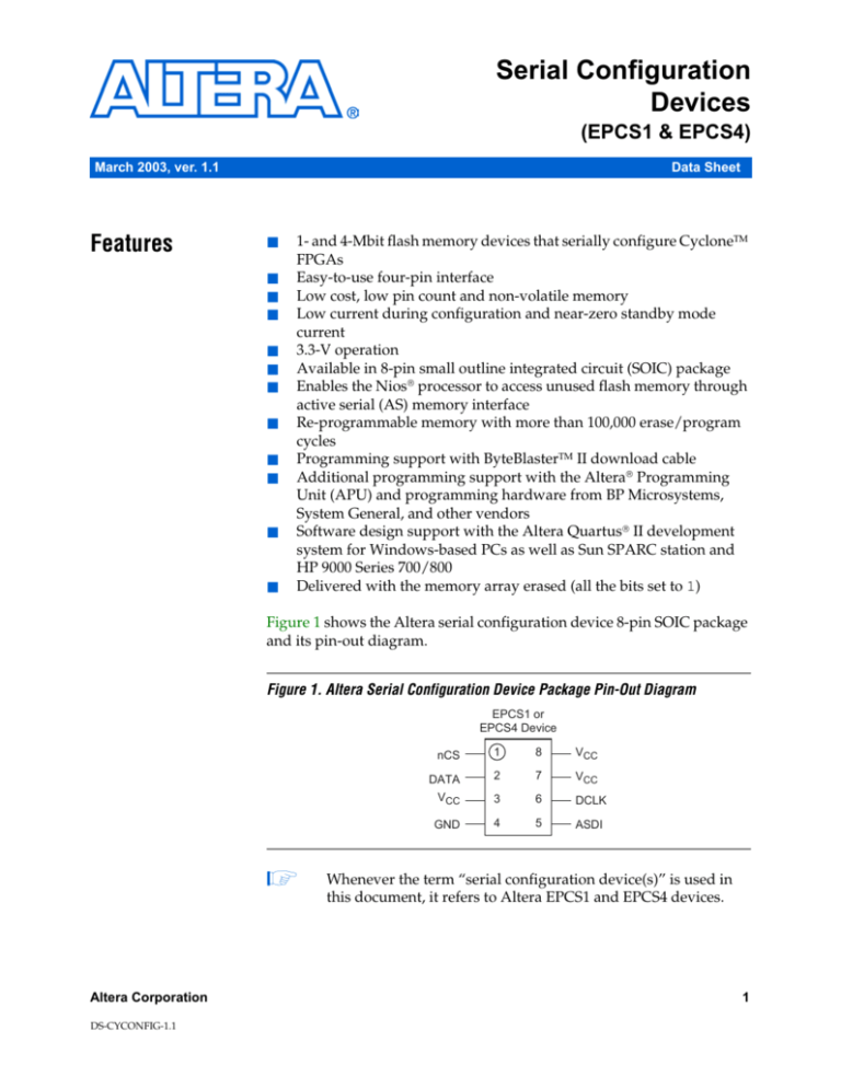
Figure 1 shows the Altera serial configuration device 8-pin SOIC package
and its pin-out diagram.
Figure 1. Altera Serial Configuration Device Package Pin-Out Diagram
EPCS1 or
EPCS4 Device
1
Altera Corporation
DS-CYCONFIG-1.1
nCS
1
8
VCC
DATA
VCC
2
7
VCC
3
6
DCLK
GND
4
5
ASDI
Whenever the term “serial configuration device(s)” is used in
this document, it refers to Altera EPCS1 and EPCS4 devices.
1
Serial Configuration Devices (EPCS1 & EPCS4) Data Sheet
Functional
Description
With SRAM-based devices such as Cyclone FPGAs, configuration data
must be reloaded each time the system initializes, or when a new
configuration is needed. Serial configuration devices are flash memory
devices with a serial interface that can store configuration data for a
Cyclone device and reload the data to the device upon power-up or
reconfiguration. Table 1 lists the serial configuration devices.
Table 1. Serial Configuration Devices (3.3-V Operation)
Device
Memory Size (Bits)
EPCS1
1,048,576
EPCS4
4,194,304
Table 2 lists the serial configuration device used with each Cyclone FPGA
and the configuration file size.
Table 2. Serial Configuration Device for Cyclone Devices
Cyclone Device
Configuration
File Size
(Mbits) (1)
Serial Configuration Device
EPCS1
EPCS4
EP1C3
0.628
v
v
EP1C4
0.925
v
v
EP1C6
1.167
v
EP1C12
2.324
v
EP1C20
3.559
v
v
Note to Table 2:
(1)
These are preliminary, uncompressed file sizes.
With the new data-decompression feature in the Cyclone FPGA family,
designers can use smaller serial configuration devices to configure larger
Cyclone FPGAs. Serial configuration devices cannot be cascaded.
f
See AN 250: Configuring Cyclone FPGAs for more information regarding
the Cyclone FPGA decompression feature in AS mode.
The serial configuration devices are designed to configure Cyclone FPGAs
and cannot configure other existing device families. Figure 2 shows the
serial configuration device block diagram.
2
Altera Corporation
Serial Configuration Devices (EPCS1 & EPCS4) Data Sheet
Figure 2. Serial Configuration Device Block Diagram
Serial Configuration Device
nCS
Control
Logic
DCLK
DATA
I/O Shift
Register
Accessing
Memory in
Serial
Configuration
Devices
f
Altera Corporation
Address Counter
Data Buffer
Decode Logic
Memory
Array
ASDI
Status Register
A designer can access the unused memory locations of the serial
configuration device through the Nios processor and SOPC Builder to
store/retrieve data or configuration files. SOPC Builder is an Altera tool
for creating bus-based (especially microprocessor-based) systems in
Altera devices. SOPC Builder assembles library components like
processors and memories into custom microprocessor systems.
SOPC Builder includes an interface core specifically for the serial
configuration device. Using this core, a designer can create a system with
a Nios embedded processor that allows software access to any memory
location within the serial configuration device.
For more information on accessing memory within the serial
configuration device, contact Altera Applications.
3
Serial Configuration Devices (EPCS1 & EPCS4) Data Sheet
Pin Description
As shown in Figure 1, the serial configuration device is an 8-pin device.
The control pins on the serial configuration device are: serial data output
(DATA), active serial data input (ASDI), serial clock (DCLK), and chip select
(nCS). Table 3 shows the serial configuration device’s pin descriptions.
Table 3. Serial Configuration Device Pin Description
Pin Name
Pin Number
Pin Type
Description
DATA
2
Output
DATA output signal transfers the data serially out of the serial
configuration device into the Cyclone FPGA during
read/configuration operation. During a read/configuration operation,
the serial configuration device is enabled by pulling nCS low. The
DATA signal transitions on the falling edge of DCLK.
ASDI
5
Input
Active serial data input signal is used to transfer data serially into the
serial configuration device. It receives the data that should be
programmed into the serial configuration device. Values register on
the rising edge of DCLK.
nCS
1
Input
Active low chip select input signal toggles at the beginning and end
of a valid instruction. When this signal is high, the device is
deselected and the DATA signal is tri-stated. When the signal is low,
it enables the device and puts the device in an active mode. After
power up, the serial configuration device requires a falling edge on
the nCS signal before beginning any operation.
DCLK
6
Input
DCLK is provided by the Cyclone FPGA. This signal provides the
timing of the serial interface. The data presented at ASDI are latched
in to the serial configuration device, at the rising edge of DCLK. Data
on the DATA pin changes after the falling edge of DCLK and is latched
into the Cyclone FPGA on the rising edge.
VCC
3, 7, 8
Power
Power pins connect to 3.3 V.
GND
4
Ground
Ground pin.
Programming
& Configuration
File Support
The Quartus II design software provides programming support for serial
configuration devices. After selecting the serial configuration device, the
Quartus II software automatically generates the Programmer Object File
(.pof) to program the device. The software allows users to select the
appropriate serial configuration device density that most efficiently stores
the configuration data for a selected Cyclone FPGA.
Serial configuration devices are programmed using the APU with the
appropriate programming adapter (PLMSEPC-8) via the Quartus II
software or the ByteBlaster II download cable via the Quartus II software.
In addition, many third-party programmers, such as BP Microsystems
and System General, offer programming hardware that supports serial
configuration devices.
4
Altera Corporation
Serial Configuration Devices (EPCS1 & EPCS4) Data Sheet
During in-system programming of a serial configuration device via the
ByteBlaster II download cable, the cable pulls nCONFIG low to reset the
Cyclone device and overrides the 10-kΩ pull-down resistors on the
Cyclone device’s nCE pin (see Figure 5). The download cable then uses the
four interface pins (DATA, nCS, ASDI, and DCLK) to program the serial
configuration device memory. Once the programming is complete, the
download cable releases the serial configuration device’s four interface
pins and the Cyclone device’s nCE pin, and pulses nCONFIG to start
configuration.
Figure 3 shows the timing waveform for write operation to the serial
configuration device.
Figure 3. Write Operation Timing
tCSH
nCS
tNCSH
tNCSSU
tCH
tCL
DCLK
tDSU
ASDI
DATA
tDH
Bit n
Bit n − 1
Bit 0
High Impedance
Altera Corporation
5
Serial Configuration Devices (EPCS1 & EPCS4) Data Sheet
Table 4 defines the serial configuration device timing parameters for write
operation.
Table 4. Write Operation Parameters
Symbol
Parameter
Min
fWCLK
Write clock frequency (from
Cyclone FPGA or ByteBlaster II
cable)
Max
Unit
20
MHz
tCH
DCLK high time
25
ns
tCL
DCLK low time
25
ns
tNCSSU
Chip select (nCS) setup time
10
ns
tNCSH
Chip select (nCS) hold time
10
ns
tDSU
Data (ASDI) in setup time
before rising edge on DCLK
5
ns
tDH
Data (ASDI) hold time after
rising edge on DCLK
5
ns
tCSH
Chip select high time
100
ns
Figure 4 shows the timing waveform for the serial configuration device's
read operation.
Figure 4. Read Operation Timing
nCS
tCH
DCLK
tCL
tnCLK2D
Bit N
DATA
ASDI
6
Bit N − 1
tODIS
Bit 0
Add_Bit 0
Altera Corporation
Serial Configuration Devices (EPCS1 & EPCS4) Data Sheet
Table 5 defines the serial configuration device timing parameters for read
operation.
Table 5. Read Operation Parameters
Symbol
f
fRCLK
Read clock frequency (from
Cyclone FPGA)
Altera Corporation
Min
Max
Unit
20
MHz
tCH
DCLK high time
25
ns
tCL
DCLK low time
25
ns
tODIS
Output disable time after read
15
ns
tnCLK2D
Clock falling edge to data
15
ns
For more information on programming and configuration support, see the
following documents:
■
■
■
Cyclone FPGA
Configuration
Parameter
Altera Programming Hardware Data Sheet
Programming Hardware Manufacturers
ByteBlaster II Parallel Port Download Cable Data Sheet
Cyclone FPGAs can be configured with a serial configuration device
through AS configuration mode. There are four signals on the serial
configuration device that interface directly with the Cyclone device’s
control signals. The serial configuration device signals DATA, DCLK, ASDI,
and nCS interface with DATA0, DCLK, ASDO, and nCSO control signals on
a Cyclone FPGA, respectively. Figure 5 shows a serial configuration
device programmed via a download cable configuring a Cyclone FPGA in
AS mode. Figure 6 shows a serial configuration device programmed using
the APU or a third-party programmer configuring a Cyclone FPGA in AS
configuration mode.
7
Serial Configuration Devices (EPCS1 & EPCS4) Data Sheet
Figure 5. Cyclone Configuration in AS Mode (Serial Configuration Device Programmed Using Download
Cable)
VCC (1)
10 kΩ
VCC (1) VCC (1)
10 kΩ
10 kΩ
Cyclone FPGA
CONF_DONE
nSTATUS
Serial
Configuration
Device (2)
nCEO
nCONFIG
nCE
MSEL[1..0]
00
(3)
10 kΩ
DATA
DATA0
DCLK
DCLK
nCS
nCSO
ASDI
ASDO
Pin 1
8
VCC (1)
Altera Corporation
Serial Configuration Devices (EPCS1 & EPCS4) Data Sheet
Figure 6. Cyclone Configuration in AS Mode (Serial Configuration Device Programmed by APU or Third-Party
Programmer)
VCC (1)
10 kΩ
VCC (1) VCC (1)
10 kΩ
10 kΩ
Cyclone FPGA
CONF_DONE
nSTATUS
Serial
Configuration
Device (2)
nCEO
nCONFIG
nCE
DATA
DATA0
DCLK
DCLK
nCS
nCSO
ASDI
ASDO
MSEL[1..0]
00
(3)
Notes to Figures 5 and 6:
(1)
(2)
(3)
VCC = 3.3 V.
Serial configuration devices cannot be cascaded.
Set MSEL0 to 0 and MSEL1 to 0 for AS configuration mode.
The Cyclone FPGA acts as the configuration master in the configuration
flow and provides the DCLK to the serial configuration device. The
Cyclone device enables the serial configuration device by pulling the nCS
signal low via the nCSO signal (See Figures 5 and 6). Consequently, the
Cyclone FPGA sends the instructions and addresses to the serial
configuration device via the ASDO signal. The serial configuration device
responds to the instructions by sending the configuration data to the
Cyclone FPGA’s DATA0 pin on the falling edge of DCLK. The data is
latched into the Cyclone device’s DCLK signal’s rising edge.
The Cyclone FPGA controls the nSTATUS and CONF_DONE pins during
configuration in AS mode. If the CONF_DONE signal does not go high at
the end of configuration or if the signal goes high too early, the Cyclone
FPGA will pulse its nSTATUS pin low to start reconfiguration. Upon
successful configuration, the Cyclone FPGA releases the CONF_DONE pin,
allowing the external 10-kΩ resistor to pull this signal high. Initialization
begins after the CONF_DONE goes high and completes within 136 clock
cycles. After initialization, the Cyclone FPGA enters user mode.
f
Altera Corporation
For more information on configuring Cyclone FPGAs in AS mode or other
configuration modes, see AN 250: Configuring Cyclone FPGAs.
9
Serial Configuration Devices (EPCS1 & EPCS4) Data Sheet
Serial configuration devices cannot be cascaded. Therefore, when a design
requires multiple Cyclone FPGAs, the Cyclone FPGAs are configured by
a single serial configuration device. Check Table 1 to ensure the
programming file size of the cascaded Cyclone FPGAs does not exceed the
capacity of a serial configuration device. Designers can choose any serial
configuration device according to the system requirements. Figure 7
shows the AS configuration scheme with multiple Cyclone FPGAs in the
chain. In AS configuration mode, all the devices in the chain must be
Cyclone devices.
Figure 7. Multiple Devices in AS Mode
VCC (1)
10 kΩ
VCC (1)
VCC (1)
10 kΩ
10 kΩ
Cyclone FPGA (Master) (2)
Serial
Configuration
Device (3)
Cyclone FPGA (Slave) (2)
CONF_DONE
CONF_DONE
nSTATUS
nSTATUS
nCONFIG
nCONFIG
nCE
nCEO
MSEL[1..0]
nCE
00
(4)
nCEO
MSEL[1..0]
DATA
DATA0
DATA0
DCLK
DCLK
DCLK
nCS
nCSO
ASDI
ASDO
01
(5 )
Notes to Figure 7:
(1)
(2)
(3)
(4)
(5)
VCC = 3.3 V.
In AS mode, the first Cyclone device in the chain is the master device. The other Cyclone devices in the chain are
slave devices and must be in passive serial (PS) configuration mode.
Serial configuration devices cannot be cascaded.
Set MSEL0 to 0 and MSEL1 to 0 to select AS mode in the Cyclone device.
Set MSEL0 to 0 and MSEL1 to 1 to select PS mode in the Cyclone device.
Figure 8 shows the timing waveform for Cyclone FPGA AS configuration
scheme using a serial configuration device.
10
Altera Corporation
Serial Configuration Devices (EPCS1 & EPCS4) Data Sheet
Figure 8. AS Configuration Timing
tPOR
nCONFIG
nSTATUS
CONF_DONE
nCSO
tCL
DCLK
tCH
tH
ASDO
Read Address
tSU
bit N
DATA0
bit N − 1
bit 1
bit 0
136 Cycles
INIT_DONE
User Mode
User I/O
Table 6 shows the timing parameters for AS configuration mode.
Table 6. Timing Parameters for AS Configuration
Symbol
Parameter
Min
Typ
Max
Unit
15
20
MHz
fCLK
DCLK frequency (from Cyclone FPGA)
tCH
DCLK high time
25
tCL
DCLK low time
25
ns
tH
Data hold time after rising edge on DCLK
0
ns
tSU
Data set up time before rising edge on DCLK
5
tPOR
POR delay
Power &
Operation
Altera Corporation
ns
ns
100
ms
This section describes the power modes, power-on reset (POR) delay,
error detection, and initial programming state of serial configuration
devices.
11
Serial Configuration Devices (EPCS1 & EPCS4) Data Sheet
Power Mode
Serial configuration devices support active power and standby power
modes. When nCS is low, the device is enabled and is in active power
mode. The Cyclone FPGA is configured while in active power mode.
When nCS is high, the device is disabled but could remain in active power
mode until all internal cycles have completed (such as program or erase
operations). The serial configuration device then goes into stand-by
power mode. The ICC1 parameter specifies the VCC supply current when
the device is in active power mode and the ICC0 parameter specifies the
current when the device is in stand-by power mode (see Table 10).
Power-On Reset
During initial power-up, a POR delay occurs to help stabilize the system
voltage levels. In AS configuration, the Cyclone FPGA controls the
configuration and has a longer POR delay than the serial configuration
device. Therefore, the POR delay is governed by the Cyclone FPGA
(typically 100 ms).
Error Detection
In AS configuration with the serial configuration device, the Cyclone
FPGA monitors the configuration status through the nSTATUS and
CONF_DONE pins. If an error condition occurs (nSTATUS driven low) or if
the CONF_DONE pin does not go high, the Cyclone FPGA will initiate
reconfiguration by pulsing the nSTATUS and nCSO signals, which
controls the chip select pin on the serial configuration device (nCS).
After an error, configuration automatically restarts if the Auto-Restart
Upon Frame Error option is turned on in the Quartus II software.
12
Altera Corporation
Serial Configuration Devices (EPCS1 & EPCS4) Data Sheet
Operating
Conditions
Tables 6 through 10 provide information on absolute maximum ratings,
recommended operating conditions, DC operating conditions, and
capacitance for serial configuration devices.
Table 7. Absolute Maximum Ratings
Symbol
Note (1)
Parameter
Condition
Min
Max
Unit
V
VCC
Supply voltage
With respect to ground
−0.6
4.0
VI
DC input voltage
With respect to ground
−0.6
4.0
V
IMAX
DC VCC or GND current
15
mA
IOUT
DC output current per pin
−25
25
mA
PD
Power dissipation
54
mW
TSTG
Storage temperature
No bias
−65
150
°C
TAMB
Ambient temperature
Under bias
−65
135
°C
TJ
Junction temperature
Under bias
135
°C
Table 8. Recommended Operating Conditions
Symbol
Parameter
Conditions
Min
Max
Unit
VCC
Supply voltage
(2)
3.0
3.6
V
VI
Input voltage
Respect to GND
−0.3
0.3 + VCC
V
VO
Output voltage
0
VCC
V
TA
Operating temperature
0
70
°C
−40
85
°C
For commercial use
For industrial use
tR
Input rise time
5
ns
tF
Input fall time
5
ns
Table 9. DC Operating Conditions
Symbol
Parameter
VIH
High-level input voltage
Conditions
VIL
Low-level input voltage
VOH
High-level output voltage
IOH = −100 µA (3)
Min
Max
Unit
0.7 × VCC
VCC + 0.4
V
−0.5
0.3 × VCC
VCC − 0.2
V
V
VOL
Low-level output voltage
IOL = 1.6 mA (3)
0.4
V
II
Input leakage current
VI = VCC or GND
−10
10
µA
IOZ
Tri-state output off-state current
VO = VCC or GND
−10
10
µA
Altera Corporation
13
Serial Configuration Devices (EPCS1 & EPCS4) Data Sheet
Table 10. ICC Supply Current
Symbol
Parameter
ICC0
VCC supply current (standby)
ICC1
VCC supply current (during active
power mode)
Table 11. Capacitance
Symbol
Conditions
Min
Max
Unit
50
µA
5
14
mA
Min
Note (4)
Max
Unit
CIN
Input pin capacitance
Parameter
VIN = 0 V
Conditions
6
pF
COUT
Output pin capacitance
VOUT = 0 V
8
pF
Notes to Tables 7 − 11:
(1)
(2)
(3)
(4)
See the Operating Requirements for Altera Devices Data Sheet.
Maximum VCC rise time is 100 ms.
The IOH parameter refers to high-level TTL or CMOS output current; the I OL parameter refers to low-level TTL or
CMOS output current.
Capacitance is sample-tested only at TA = 25 °C and at a 20-MHz frequency.
Package
All serial configuration devices are available in 8-pin plastic SOIC
package. Figure 9 shows the mechanical drawing and specifications for
this package.
f
14
For more information on Altera device packaging, see the Altera Device
Package Information Data Sheet.
Altera Corporation
Serial Configuration Devices (EPCS1 & EPCS4) Data Sheet
Figure 9. 8-Pin SOIC Serial Configuration Device Package
Notes (1), (2)
N
H E
Pin 1
D
h × 45
o
Seating
Plane
A
A1
e
B
8
C
L
Symbol
A
A1
B
C
D
E
e
H
h
L
N
Dimentions (mm)
Min.
_
_
_
_
_
_
_
_
_
8
_
Nom.
1.35
0.10
0.33
0.19
4.80
3.80
1.27 BSC
5.80
0.25
0.40
8
o
0 C
Max.
1.75
0.25
0.51
0.25
5.00
4.00
6.20
0.50
0.90
o
8 C
Notes to Figure 9:
(1)
(2)
Ordering Code
All dimensions and tolerances conform to ANSI Y14.5M - 1982.
JEDEC reference MS-013 option AE.
Table 12 shows the ordering codes for serial configuration devices.
Table 12. Serial Configuration Device Ordering Codes
Altera Corporation
Device
Ordering Code
EPCS1
EPCS1SI8
EPCS4
EPCS4SI8
15
Serial Configuration Devices (EPCS1 & EPCS4) Data Sheet
101 Innovation Drive
San Jose, CA 95134
(408) 544-7000
http://www.altera.com
Applications Hotline:
(800) 800-EPLD
Literature Services:
lit_req@altera.com
16
Copyright © 2003 Altera Corporation. All rights reserved. Altera, The Programmable Solutions Company, the
stylized Altera logo, specific device designations, and all other words and logos that are identified as
trademarks and/or service marks are, unless noted otherwise, the trademarks and service marks of Altera
Corporation in the U.S. and other countries. All other product or service names are the property of their
respective holders. Altera products are protected under numerous U.S. and foreign patents and pending
applications, maskwork rights, and copyrights. Altera warrants performance of its
semiconductor products to current specifications in accordance with Altera's standard
warranty, but reserves the right to make changes to any products and services at any time
without notice. Altera assumes no responsibility or liability arising out of the application
or use of any information, product, or service described herein except as expressly agreed
to in writing by Altera Corporation. Altera customers are advised to obtain the latest
version of device specifications before relying on any published information and before
placing orders for products or services.
Altera Corporation
