Photovoltaics Information Brief No.1
D. Garlovsky and W. Pickin
1
Schools & Homes Energy Education Project
PLUGGING into the
sun
Renewable
Energy Education
SOLAR CELLS
A solar cell is an electronic device that produces electricity when light falls on it. The light is
absorbed and the cell produces dc voltage and current. The device has a positive and a
negative contact between which the voltage is generated and through which the current can
flow. You connect these contacts to whatever it is you want to power. Solar cells have no
moving parts. Effectively they take light energy and convert it into electrical energy in an
electrical circuit, exploiting a physical process known as the photovoltaic effect.
The discovery of the photovoltaic effect is credited to the French physicist, Edmond
Becquerel, in 1839. He found that by concentrating the sun's light on one side of a battery the
output current of the battery could be increased. This revolutionary discovery triggered the
idea that one could produce energy from light by an artificial process. In 1883 an American
inventor produced a solar cell from a material called selenium, but it was very inefficient.
Selenium became used in light-exposure meters for cameras, but not for power production.
It was not until the 1950s that practical solar cells were developed. In 1948 the transistor was
invented, at Bell Laboratories in the United States, and it was found that the same high
quality silicon wafers used for making transistors could be used to make solar cells. This
work was published in 1954. From 1958 onwards the cells were employed in the space race.
Solar cells are still the only sensible source of electrical power for space satellites, because
they are in effect batteries that never run out.
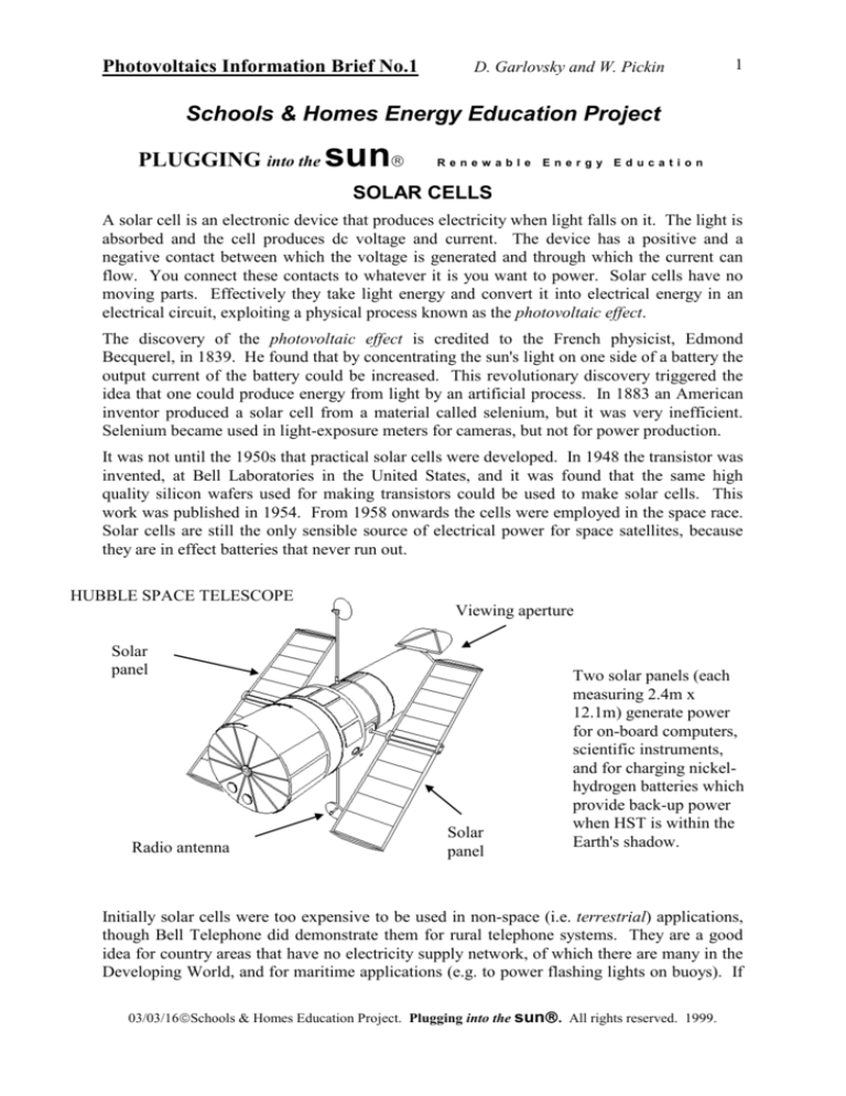
HUBBLE SPACE TELESCOPE
Viewing aperture
Solar
panel
Radio antenna
Solar
panel
Two solar panels (each
measuring 2.4m x
12.1m) generate power
for on-board computers,
scientific instruments,
and for charging nickelhydrogen batteries which
provide back-up power
when HST is within the
Earth's shadow.
Initially solar cells were too expensive to be used in non-space (i.e. terrestrial) applications,
though Bell Telephone did demonstrate them for rural telephone systems. They are a good
idea for country areas that have no electricity supply network, of which there are many in the
Developing World, and for maritime applications (e.g. to power flashing lights on buoys). If
03/03/16Schools & Homes Education Project. Plugging into the sun. All rights reserved. 1999.
Photovoltaics Information Brief No.1
D. Garlovsky and W. Pickin
2
cells can be made cheap enough (and great efforts are being made to achieve this) they could
even replace our normal methods of making electricity, which are either polluting and/or nonrenewable (burning fossil fuels) or waste poses a long term environmental hazard (radioactive
waste from nuclear power plants). Solar cells produce no emissions and do not contribute to
the greenhouse effect, and the amount of energy available from the world's sunlight is far
more than we should ever need.
Individual solar cells are small and therefore not very powerful (though they can run
calculators and watches). More powerful supplies can be made by connecting many cells
together in a solar module. Modules are connected together to form solar panels, and in turn
panels are connected together to form solar arrays.
Efficiency
The efficiency of a solar cell is a measure of the proportion of the light hitting it that is
actually converted into electricity. If the cell were 100% efficient then it would turn all the
incident light into energy, but sadly this is impossible: the maximum allowed within the laws
of physics is between 30% and 40%. Practical solar cells made from silicon wafers
(monocrystalline silicon) can have an efficiency of 16% or so. Thin-film solar cells (e.g.
amorphous silicon solar cells) have lower efficiencies than this, at least for commercial cells,
but are much cheaper to produce.
Around mid-day on a clear summer's day the sunlight falling on the earth has a power density
of about 1 kW (1000 watts) for every square meter of surface; (this is typically the power
given off by a one-bar electric fire). A solar module measuring 0.30 m × 0.45 m has an area
of 0.135 m², and therefore when you point it at the sun the light falling on it has a power of
0.135 × 1000 watts = 135 watts. If the module is 10% efficient, the power available from it is
10% of this, i.e. 13.5 watts. The module is stated to have an output of 13.5 watts peak, i.e. at
the peak sunlight of 1000 watts per square meter. The output will be less at other times of the
day, in cloudy conditions, or if the module is in the shade or not pointing directly at the sun.
In space the output is higher because the solar radiation there is stronger, not being affected
by the earth’s atmosphere. It has a power density of 1365 watts per square metre.
How does the light intensity effect the solar cell?
As the intensity of light falls, because of clouds or time of day, solar cell output also falls.
The cell's current is more sensitive to the light intensity than the voltage is. Roughly speaking
if you halve the light intensity you halve the current; but the voltage falls only slightly.
The light intensity can also be reduced just by twisting the cell. The output of a solar cell is at
its maximum when it is perpendicular to the incident light beam, i.e. when it is pointed at the
sun. If you now change the angle, the cell intercepts less of the light beam; however, this
smaller amount of light is still spread out over the same area of cell, so the light intensity on
the cell is reduced.
03/03/16Schools & Homes Education Project. Plugging into the sun. All rights reserved. 1999.
Photovoltaics Information Brief No.1
D. Garlovsky and W. Pickin
3
INSIDE A SOLAR CELL - HOW DOES IT WORK?
Photons
Photons are what make up the light we see. Light is an electromagnetic wave that is
transmitted in tiny pulses of energy. These tiny pulses of energy are referred to as photons.
Semiconductors
All substances can be arranged in order of their ability to conduct electrical charges. Those at
the top of the list are called conductors, and those at the bottom are called insulators.
Whether a substance is classified as a conductor or an insulator depends on it’s interatomic
bonding and on how tightly the atoms of the substance hold their electrons. The interatomic
bonding in some materials, such as silicon, is intermediate between that of a good conductor
and that of a good insulator.
Rubber, glass, wood
Poor conductors
Good insulators
Silicon, germainium
Semi-conductors
Copper, iron,
aluminium, gold
Good conductors
Poor insulators
Most metals are good conductors, most non-metals are poor conductors.
Silicon and germanium belong to group of materials called semiconductors. They are good
insulators in their pure crystalline form at very low temperature. Conductivity increases with
temperature or when they are exposed to light Conductivity can be increased tremendously
when even one atom in ten million is replaced with an impurity that adds or removes an
electron from the crystal structure. The chips used in electronics are made of semiconductor
materials, and so are photovoltaic cells. The most common semiconductor is silicon.
Semiconductor materials will also interact with light (see Figure 1). A photon hitting a
silicon atom can give an electron within the atom enough energy to leave it and move off
through the structure. The negatively charged electron leaves a positively charged hole (a
position once occupied by an electron) in its place; so the photon has created an electron/hole
pair. An electron orbiting a surrounding atom near to a hole can move into the hole leaving a
new hole in it's place; in this way the positively charged holes can also move through the
structure. In the presence of an electric field the electrons move in one direction and the holes
in the other, because they have opposite electric charges with holes behaving in nearly all
respects as positive particles. In semiconductor materials, electric current is the flow of
oppositly charged electrons and holes.
The Photovoltaic (PV) Effect
Without an electric field to separate the electrons and holes created by the light they would
soon recombine and there would be no net current. To avoid this a photovoltaic cell (PV cell)
is a wafer or thin film of semiconductor material which is arranged to have an internal electric
field, pointing from the top surface of the wafer or film to the bottom surface (or vice versa).
An electrical contact, usually aluminium, covers the bottom surface. The top surface also has
an electrical contact, but this one is transparent so as to let in the light. When the silicon (or
03/03/16Schools & Homes Education Project. Plugging into the sun. All rights reserved. 1999.
Photovoltaics Information Brief No.1
D. Garlovsky and W. Pickin
4
other semiconductor material) in the PV cell absorbs light, electron/hole pairs are generated.
Because of the internal electric field the electrons move to one contact and holes to the other
thus building up a voltage. The cell acts as a voltage source. If you connect the two contacts
with a wire an electric current will flow in the wire; this is known as the "short-circuit
current" of the PV cell; you can measure it with an ammeter. If you don't connect the
contacts the electrons and holes build up on opposite surfaces of the cell, producing a voltage
between the contacts that you can measure with a voltmeter; this is called the "open-circuit
voltage" of the PV cell.
The internal field; p-n junctions
To produce the necessary internal electric field we make use of two types of "doped"
semiconductor material; these are called "n-type" and "p-type" material.
n-type silicon contains a small percentage of phosphorus atoms. These fit quite well into the
structure of the silicon, except that each has one more electron than each silicon atom. These
extra electrons escape from the phosphorus and are free to move round the structure; what
they leave behind are positively charged phosphorus ions, (which are fixed in the structure
and can't move). The phosphorus is called an n-type dopant because of the negative electrons
it adds to the silicon; the resulting material is called n-type silicon because of the electrons it
contains (though you should remember it contains an equal number of positive fixed charges).
p-type silicon contains boron atoms. These fit quite well into the structure of the silicon,
except that each has one fewer electrons than each silicon atom. They therefore grab
electrons from the silicon, creating holes that are free to move round the structure; what the
holes leave behind are negatively charged boron ions, (because of the extra electron they've
grabbed); the boron ions are fixed in the structure and can't move. The material is called ptype because of the positive holes it contains; it also contains an equal number of negative
fixed charges. Boron is said to be a p-type dopant in silicon.
Now consider a wafer of silicon that has excess boron in the top half (p-type silicon) and
excess phosphorus in the bottom half (n-type silicon). In the middle there is what is called a
pn-junction, where the material changes from p-type to n-type. On the n-type side of the
junction there will be electrons and fixed positive charge (phosphorus ions); on the p-type
side there will be holes and fixed negative charge (boron ions). Because there are many
electrons in n-type and very few in p-type material the electrons from the n-side will tend to
spread into the p-side, leaving some net positive charge on the n-side (because of the positive
phosphorus ions); this positive charge will stop the electrons diffusing too far into the p-type
material and is further increased by holes spreading from the p-side, (which also leaves
negative charge on the p-side, because of the negative boron ions). The result is fixed
positive electric charges on the n-type side of the junction and negative fixed charges on the
p-type side. This produces an internal electric field pointing across the junction, which is
precisely what is needed for a PV cell.
This accelerates electrons from electron-hole pairs separated by light from the p-type material
into the n-type material where there are many electrons and few holes and so not much
chance of recombining. Similarly the junction accelerates holes from electron-hole pairs in
the n-type material to the p-type material where they are similarly unlikely to recombine.
03/03/16Schools & Homes Education Project. Plugging into the sun. All rights reserved. 1999.
Photovoltaics Information Brief No.1
5
D. Garlovsky and W. Pickin
Solar cells
A solar cell is a PV cell designed to convert sunlight to electricity. The simplest cells (Figure
1a) consist of a circular silicon wafer with a pn-junction sandwiched in the middle, a metallic
bottom contact (e.g. aluminium) and a transparent top contact (either a transparent conducting
oxide or a grid-like metal structure). Solar panels with cells like this have played a vital role
in space technology since the late '50s, powering space satellites. They are expensive to
produce because silicon wafers are expensive to produce (mainly because they are high-purity
single crystals) but their cost was unimportant in the space race.
Photon
Photon
Photon
FRONT CONTACT GRID
hole
SILICON CONTAINING BORON AS DOPANT
p-region
hole
Figure 1a. crystalline
silicon PV cell
electron
SILICON CONTAINING PHOSPHOROUS AS DOPANT
electron
n-region
BACK CONTACT PLATE
In recent years there has been a continuous search for cheaper forms of PV cell, economical
enough to be used in applications here on earth (terrestrial applications). Attempts have been
made to use cheaper forms of silicon, of lower quality than that used in computer chips,
despite the poorer cell efficiencies that result. One possibility has been to replace the singlecrystal wafer by polycrystalline squares, (consisting of many small grains of crystalline
material). A more radical approach is to use amorphous silicon, having no crystalline
structure at all. This material has the advantage of being much more light-absorbing than
crystalline silicon: a thin film on a suitable substrate only a few microns thick (a thousandth
of a millimetre) absorbs most of the sunlight falling on it; by contrast crystalline cells have to
be about 100 microns and in practice are 0.5mm thick. This means that you need far less
amorphous silicon to make the cells, and they can even be made flexible, whereas crystalline
cells are very fragile. The electrons and holes don't move so easily in amorphous silicon, but
this is partly compensated for by the fact that they don't have to move as far (because the cell
is so thin). Cell efficiencies are perhaps only half those in crystalline silicon, but the
amorphous cells potentially cost much less than half for the same surface area, so they seem
to be the most economical choice at the moment.
Manufacture of amorphous silicon solar cells
The manufacture of amorphous silicon cells (e.g. by UNI-SOLAR) is very different from
that of crystalline cells. No wafers are involved. Instead the silicon is deposited as a thin
film on a substrate, usually either stainless steel or a glass sheet covered with a layer of tin
oxide acting as a transparent contact.
03/03/16Schools & Homes Education Project. Plugging into the sun. All rights reserved. 1999.
Photovoltaics Information Brief No.1
D. Garlovsky and W. Pickin
6
As shown in Figure 2, the substrate is placed in a steel chamber which is evacuated (i.e. all
the air is pumped out); a small amount of the gas silane (a gaseous compound of silicon and
hydrogen) is then bled in through a valve. Two metal plates within the chamber connect to a
radio-frequency power supply which sets up a purple-coloured glow discharge (sometimes
called a plasma) in the silane gas; electrons collide with silane molecules and knock away the
hydrogen atoms, leading to the silicon atoms depositing in a thin amorphous film on the
substrate (mixed with some of the hydrogen atoms, which in fact turn out to be beneficial for
the cell). Substrates used are often 300 mm wide, but in principle they could be larger,
limited only by the size of the deposition chamber.
To make n-type amorphous silicon the same procedure is followed, except that the silane is
mixed with one or two per cent of the gas phosphine, a compound of phosphorus and
hydrogen. To make p-type amorphous silicon the silane is mixed with diborane, a compound
of boron and hydrogen. Either separate chambers or sequential gas streams are used for
making each type.
Photon
Photon
Figure 1b:
amorphous silicon
PV cell
SUPERSTRATE (not necessary if stainless steel back contact used)
Transparent front contact (tin oxide or indium-tin oxide)
AMORPHOUS SILICON CONTAINING BORON
p-layer
Photon
INTRINSIC
LAYER
hole
n-layer
electron
electron
hole
AMORPHOUS SILICON
AMORPHOUS SILICON CONTAINING PHOSPHOROUS
Aluminium back contact or stainless steel
03/03/16Schools & Homes Education Project. Plugging into the sun. All rights reserved. 1999.
Photovoltaics Information Brief No.1
D. Garlovsky and W. Pickin
7
Unfortunately electron-hole recombination of n- or p-type amorphous silicon to light is very
high. To get round this problem the cell is made mostly from undoped amorphous silicon
(i.e. using just silane): the thin film of undoped amorphous silicon is sandwiched between far
thinner layers of n- and p-type amorphous silicon, as shown in Figure 1b. The n- and p-layers
serve to produce the internal field across the undoped layer, but almost all the light is
absorbed in the undoped layer. (The undoped material is referred to as intrinsic, and the cell
is said to have a p-i-n structure, as opposed to the p-n structure of crystalline silicon cells).
The process used for depositing amorphous silicon lends itself well to mass production
techniques. The substrate (with its electrical contact layer if necessary) passes into a chamber
and receives the n-type deposition, then into a chamber receiving the undoped deposition, and
then to chamber receiving the p-type deposition. (This is simpler to automate than cutting
and polishing wafers).
The PV industry benefits from technological developments in other fields. The development
of silicon coated drums for colour photocopiers is now applied to the production of
continuous metal strips covered with amorphous silicon. If the substrate is flexible stainless
steel (as with Plugging into the Sun laminates) that can be wound into a large roll, it is
possible to have a continuous roll-to-roll production process for amorphous silicon solar cells,
(Figure 3). The stainless steel sheet unwinds from the supply roll and passes though cleaning
procedures and the chambers for n-type, intrinsic, and p-type deposition before reaching the
take-up roll. The resulting cells have the additional advantage of being flexible.
Many manufacturers base their cells on glass substrates. Normally tin-oxide-coated glass is
used since the tin oxide serves as a transparent contact. The p-layer is deposited, followed by
the i-layer and then the n-layer. Aluminium is deposited to form the back contact. In this
form of structure the cell is illuminated through the glass and is protected by it (it is therefore
known as a superstrate).
A single silicon solar cell produces an open-circuit voltage of about 0.5volt. There are
amorphous silicon solar modules that are in fact single cells, producing a low voltage and a
correspondingly high current. However, it is far more common for the module to be divided
into individual strip-shaped cells, which are arranged to be connected in series to produce a
working voltage of around 14 volts, suitable for charging 12-volt lead-acid batteries.
03/03/16Schools & Homes Education Project. Plugging into the sun. All rights reserved. 1999.
Photovoltaics Information Brief No.1
D. Garlovsky and W. Pickin
8
We have dealt with the main principles of amorphous silicon solar cell production. There is a
mass of subsidiary detail which is too extensive to cover here. Cell efficiencies can be
increased to some extent by including a second p-i-n structure under the first, using an alloy
of amorphous silicon with germanium. This absorbs a longer wavelength part of the solar
spectrum. This is called a tandem cell or multi-junction cell.
Spectrum-splitting
cell, constructed of
three separate p-i-n
type, amorphous
semiconductor
solar sub-cells, each
with a different
spectral response
characteristic. In
this way, the cell
can convert the
different visible and
near infrared
wavelengths of
sunlight with
optimal efficiency.
Figure 3a: How a tandem (two layer) amorphous silicon PV cell is made.
thicker intrinsic layer chamber
thicker intrinsic layer chamber
p-layer chamber
n-layer chamber
In Roll
n-layer chamber
p-layer
chamber
Out Roll
03/03/16Schools & Homes Education Project. Plugging into the sun. All rights reserved. 1999.
Photovoltaics Information Brief No.1
9
D. Garlovsky and W. Pickin
Figure 3b: How a triple (three layer) UNI-SOLAR amorphous silicon PV cell is made.
thicker intrinsic layer chamber
thicker intrinsic layer chamber
p-layer chamber
p-layer chamber
n-layer chamber
n-layer chamber
In Roll
Out Roll
n-layer chamber
p-layer chamber
thicker intrinsic layer chamber
Adding a third p-i-n structure forms a triple-junction cell. (In production terms this is just a
matter of additional chambers and their gas supplies; see Figure 3b). The right sort of
roughening of the cell surface leads to less reflection from the cell surface, and to
corresponding increases in cell efficiency. The front contact needs careful design, and the
whole cell must be suitably encapsulated and protected against the weather. If everything is
done right there is no reason why the cells should not last for thirty years or more.
03/03/16Schools & Homes Education Project. Plugging into the sun. All rights reserved. 1999.
Photovoltaics Information Brief No.1
D. Garlovsky and W. Pickin
Figure 2: Deposition of amorphous silicon
How the Plasma Chambers Work
The plasma chambers suspend the silicon and the phosphorus or boron molecules in a
gaseous state. This mixture is pushed into a chamber which has electrodes at the top and
bottom. When the electrodes are charged an electric field is produced between them. The
electric field removes some of the electrons from the mixture so creating a gas of positively
charged ions, a plasma. A stainless steel or glass sheet with an indium/tin oxide layer, is
passed into the chamber and between the electrodes. The plasma-like gas deposits charged
particles on to the uncharged surface of the steel or glass substrate. Depending upon the
chemical nature of the gaseous mixture fed into the chamber, one of the three layers which
make up the photovoltaic cell will be formed. The thickness of the layers depends on the
speed at which the substate passes through the chamber, and the size of the chamber.
Excited molecules in a
gaseous state containing:
Electrode 1
Silicon and either boron (player) or phosphrous (nlayer)
Substrate (stainless
steel or glass)
passing through
chamber
Regular layer of
deposited silicon
and >1% doping
material
Electrode 2
03/03/16Schools & Homes Education Project. Plugging into the sun. All rights reserved. 1999.
10
