Fabrication and characterisation of semiconductor ZnSe nanocrystals
advertisement
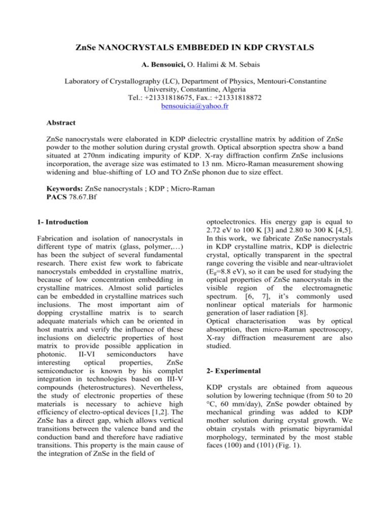
ZnSe NANOCRYSTALS EMBBEDED IN KDP CRYSTALS A. Bensouici, O. Halimi & M. Sebais Laboratory of Crystallography (LC), Department of Physics, Mentouri-Constantine University, Constantine, Algeria Tel.: +21331818675, Fax.: +21331818872 bensouicia@yahoo.fr Abstract ZnSe nanocrystals were elaborated in KDP dielectric crystalline matrix by addition of ZnSe powder to the mother solution during crystal growth. Optical absorption spectra show a band situated at 270nm indicating impurity of KDP. X-ray diffraction confirm ZnSe inclusions incorporation, the average size was estimated to 13 nm. Micro-Raman measurement showing widening and blue-shifting of LO and TO ZnSe phonon due to size effect. Keywords: ZnSe nanocrystals ; KDP ; Micro-Raman PACS 78.67.Bf 1- Introduction Fabrication and isolation of nanocrystals in different type of matrix (glass, polymer,…) has been the subject of several fundamental research. There exist few work to fabricate nanocrystals embedded in crystalline matrix, because of low concentration embedding in crystalline matrices. Almost solid particles can be embedded in crystalline matrices such inclusions. The most important aim of dopping crystalline matrix is to search adequate materials which can be oriented in host matrix and verify the influence of these inclusions on dielectric properties of host matrix to provide possible application in photonic. II-VI semiconductors have interesting optical properties, ZnSe semiconductor is known by his complet integration in technologies based on III-V compounds (heterostructures). Nevertheless, the study of electronic properties of these materials is necessary to achieve high efficiency of electro-optical devices [1,2]. The ZnSe has a direct gap, which allows vertical transitions between the valence band and the conduction band and therefore have radiative transitions. This property is the main cause of the integration of ZnSe in the field of optoelectronics. His energy gap is equal to 2.72 eV to 100 K [3] and 2.80 to 300 K [4,5]. In this work, we fabricate ZnSe nanocrystals in KDP crystalline matrix, KDP is dielectric crystal, optically transparent in the spectral range covering the visible and near-ultraviolet (Eg=8.8 eV), so it can be used for studying the optical properties of ZnSe nanocrystals in the visible region of the electromagnetic spectrum. [6, 7], it’s commonly used nonlinear optical materials for harmonic generation of laser radiation [8]. Optical characterisation was by optical absorption, then micro-Raman spectroscopy, X-ray diffraction measurement are also studied. 2- Experimental KDP crystals are obtained from aqueous solution by lowering technique (from 50 to 20 °C, 60 mm/day), ZnSe powder obtained by mechanical grinding was added to KDP mother solution during crystal growth. We obtain crystals with prismatic bipyramidal morphology, terminated by the most stable faces (100) and (101) (Fig. 1). higher. The 270 nm known as peak indicator of impurities [9,12]. 2,0 Fig. 1 KDP crystal Intensity (a.u.) 1,5 1,0 0,5 200 300 400 500 600 Wavelength (nm) Fig. 3 optical absorption spectra : 1- pure KDP(dashed line), 2- KDP doped ZnSe (solid line) The measurements of optical absorption were carried out by a spectrophotometer type Shimadzu UV-3101 PC, X-ray diffraction data were collected using BRUKER - AXS D8 diffractometer (λKα= 1.54 Å) and graphite.The micro-Raman spectra are recorded using a spectrometer Jobin-Yvon equipped with an Olympus microscope DX40 using laser wavelength 632 nm and power of 10 mW. 500 KD P Fig. 1 Crystal growth apparatus (LC) X-ray diffraction pattern (Fig. 4) of KDP pellet (X-ray incidents on the face parallel to the plane (100)) , show the appearance of KDP peaks situated at 24.16 and 49.27° relative, respectively, to the (100) and (200) planes. Furthermore, we note the appearance of a peak with low intensity situated at 28.57 °, which corresponds to (101) plane of diffraction of ZnSe nanocrystals (hexagonal structure) There has been a shift of the position of the peak because of the contraction of the parameters of ZnSe unit cell which due to size effect. Using Sherrer formula, the average size was estimated to be 13 nm. 400 300 (101) 100 (200) Zn Se KD P 200 (100) The absorption spectrum of a KDP pellet doped by ZnSe is given in figure 3 (solid line), showing of peak indicator of the impurity of the KDP in the 270 nm and according to its intensity can be deduced that there was an incorporation of impurities added to the solution for growth, and this peak is even more intense when the concentration of impurities incorporated is Intensité (u.a) 3- Results and discussion 0 21 28 35 42 49 2 (°) Fig. 4 X-ray diffraction of KDP doped ZnSe (wafer // (100) face) Acknowledgment The results of micro-Raman diffusion measurement on the KDP sample doped by ZnSe are presented in figure 5, Can be seen on the spectrum peaks with wave numbers 184, 365, and 474 cm-1. They are identical to some peaks of Raman spectrum of KDP. According to Subramony et al. [13] the prominent bands between 300and 1200 cm-1 are due to internal vibrations of the PO4 group, the bands below 200 cm-1 are lattice mode, we note the appearance of two bands with low intensity situated at 202 and 241cm-1 representing, respectively LO and TO ZnSe phonon frequencies [14], red shifting to lower wave-numbers is due to size effect (optical phonon energies of 1TO at 210 cm-1 and 1LO at 254 cm-1 for ZnSe crystal at room temperature) [14]. -1 -1 474 cm 365 cm cm cm -1 18 4 8000 24 1 cm -1 20 2 Intensity (a.u.) -1 8500 7500 200 400 600 -1 Wavenumber (cm ) Fig. 5 Micro-Raman Spectrum of KDP doped ZnSe 4- Conclusion UV-Vis absorption spectra reveal the band indicating impurity of KDP. Structural characterization by using X-ray diffraction indicates the incorporation of ZnSe nanocrystals in the host matrix of KDP. The low intensity of peak of diffraction, LO and TO phonon bands of ZnSe inform us about the low concentration of crystallites incorporated. This work has been supported by Laboratory of Crystallography of Mentouri-Constantine University (Algeria). References [1] C. D. Poweleit and L. M. Smith, B. T. Jonker, PHYSICAL REVIEW B, VOLUME 55, NUMBER 8, 1997 [2] N. Sankar and K. Ramachandran, Bull. Mater. Sci., Vol. 25, No. 4, August 2002, pp. 329–334. © Indian Academy of Sciences. [3] J. Hübner , M. Klude, D. Hommel, R. D. R. Bhat , J. E. Sipe, H. M. van Driel, and W. W. Rühle, phys. stat. sol. (b) 238, No. 3, 548– 551 (2003) [4] C. D. Poweleit, L. M. Smith and B. T. Jonker. PHYSICAL REVIEW B 15 FEBRUARY 1997-II VOLUME 55, NUMBER 8 [5] N. Kumbbojkar, S. Mahamuni, V. Leppert and S.H. Risbud, NanoStructured Mater. Vol. 10, No. 2, PP. 117-129, 1998 [6] A.J. Nelson, T. van Buuren, Eric Miller, T.A. Land, C. Bostedt, N. Franco, P.K. Whitman, P.A. Baisden, L.J. Terminello, T.A. Callcott "X-ray absorption analysis of [7] I. N. Ogorodnikov, V. A. Pustovarov, B. V. Shul’gin, et al., Opt. Spektrosk. 91, 243 (2001) [Opt.Spectrosc.91, 224 (2001)]. [8] D. Eimerl, Ferroelectrics, 72, 95, (1987). [9] N. Y. Garces, K. T. Stevens, L. E. Halliburton, M.Yan, N.P.Zaitseva, J. J. DeYoreo, Journal of Crystal Growth 225 (2001)435 –439 [10] A. Ryabov, N. Stelmakh, G. Pirogova, Y. Voronin, B. Zakharkin, 1991, Fiz.Tverd.Tela.33, 2660 –2662 . [11] E. Dieguez, A. Cintas, P. Hernandez, J. M. Cabrera, Journal of Crystal Growth 73 (1985)193. [12] I. M. Pritula, Y. N. Velikhov, Proceedings of SPIE,Vol.3793,1999 pp.202 –208. [13] J. A. Subramony, B. J. Marquardt, J. W. Macklin, B. Kahr, Chem. Mater. 1999, 11, 1312-1316. [14] Ja-Chin Jan, Shou-Yi Kuo, Sun-Bin Yin and WenFeng Hsieh¤ ,CHINESE JOURNAL OF PHYSICS VOL. 39, NO. 1 FEBRUARY 2001
