NanoImaging
advertisement
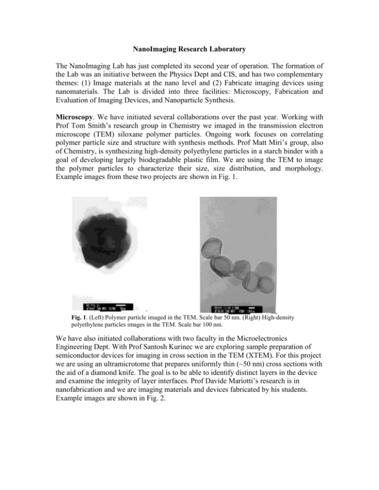
NanoImaging Research Laboratory The NanoImaging Lab has just completed its second year of operation. The formation of the Lab was an initiative between the Physics Dept and CIS, and has two complementary themes: (1) Image materials at the nano level and (2) Fabricate imaging devices using nanomaterials. The Lab is divided into three facilities: Microscopy, Fabrication and Evaluation of Imaging Devices, and Nanoparticle Synthesis. Microscopy. We have initiated several collaborations over the past year. Working with Prof Tom Smith’s research group in Chemistry we imaged in the transmission electron microscope (TEM) siloxane polymer particles. Ongoing work focuses on correlating polymer particle size and structure with synthesis methods. Prof Matt Miri’s group, also of Chemistry, is synthesizing high-density polyethylene particles in a starch binder with a goal of developing largely biodegradable plastic film. We are using the TEM to image the polymer particles to characterize their size, size distribution, and morphology. Example images from these two projects are shown in Fig. 1. Fig. 1. (Left) Polymer particle imaged in the TEM. Scale bar 50 nm. (Right) High-density polyethylene particles images in the TEM. Scale bar 100 nm. We have also initiated collaborations with two faculty in the Microelectronics Engineering Dept. With Prof Santosh Kurinec we are exploring sample preparation of semiconductor devices for imaging in cross section in the TEM (XTEM). For this project we are using an ultramicrotome that prepares uniformly thin (~50 nm) cross sections with the aid of a diamond knife. The goal is to be able to identify distinct layers in the device and examine the integrity of layer interfaces. Prof Davide Mariotti’s research is in nanofabrication and we are imaging materials and devices fabricated by his students. Example images are shown in Fig. 2. Fig. 2. (Left) Example of the cross sectional imaging we hope to achieve in the XTEM project. XTEM micrograph of hafnium oxide and molybdenum films on silicon deposited by sputtering (reactive for HfO2). The micrograph shows 6.9 nm of interfacial silicon dioxide. (Right) TEM of silicon nanocrystals. Scale bar is 50 nm. Inset is an electron diffraction pattern imaged with the TEM that confirms the material is indeed Si. Fabrication and Evaluation of Imaging Devices. We continue to build our expertise in fabrication of organic-based light-emitting devices (LEDs). Our ultimate goal is to fabricate hybrid devices in which inorganic nanocrystals are the light-emitting element and the organic layers are used for strictly electron and hole transport. A necessary prerequisite to that goal is building devices that use the organic material to emit light. These are commonly called organic light-emitting devices (OLEDs), which are further characterized on the basis of whether the devices use small molecules that are vacuum evaporated to form the device structure (SMOLEDs) or polymeric materials that are typically fabricated by spin-coating techniques (PLEDs). We are just beginning our study of PLED devices. We have made much progress in the SMOLED category and are now reproducibly fabricating devices whose optoelectronic characteristics (see bottom of Fig. 3) are consistent with those published in the scientific literature. Figure 3 shows some of our results, including a schematic cross section of the device. Holes are injected from the bottom of the device via the indium tin oxide (ITO) layer and the polymer buffer layer (PSS:PEDOT) and finally into the hole transport layer (TPD). Meanwhile electrons are injected from the top via the aluminum cathode and LiF layers into the electron transport layer (Alq3). With balanced charge injection, which is part of the optimization of the device structure, the electrons and holes meet in the Alq3 layer and form an exciton, which decays by emitting a photon (green in this device structure). We are now focused on exploring the efficiency of these devices as a function of layer position and thickness. Optimization of the thickness and placement of the LiF buffer layer is important to optimizing the device. Additionally, a study of the cathode material and thickness is critical for balancing charge injection, since it is usually the electron injection and transport that controls the balancing of charges in the device. Personnel involved: Omkar Vyavahare and Nikita Surve, both graduate students in the Materials Science & Engineering program. Fig. 3. (Upper left) Image of working display prototype. (Upper right) Schematic of device. (Lower left) I-V characteristics of device. (Lower left) Electroluminescence spectra of device. Nanocrystal Synthesis. We have a long history of synthesizing nanocrystals starting with silver halide nanocrystals (100’s of nm diameter) and have now evolved to other nanocrystals of a few or tens of nm diameter. These latter nanocrystals are composed of CeO2 and are currently intended for a nonimaging application (see Fig. 4.) These are grown by an aqueous precipitation route that is “green” and inherently scalable. The techniques we are developing can be readily applied to other compositions that have more imaging relevance. Personnel involved: Gary DiFrancesco, Associate Scientist. Project supported by Cerion Energy, Inc. number of particles size distribution mean = 2.6 +/- 0.5 nm 30 25 20 15 10 5 0 Series1 1-1.5 1.5-2 2-2.5 2.5-3 3-3.5 3.5-4 size class, nm Fig. 4. TEM image of CeO2 nanoparticles along with their size-frequency histogram. Inset is an electron diffraction pattern that confirms that the particles are CeO 2. Course and Outreach Support. The Microscopy Facility has become a popular resource for supporting various CIS/COS/COE courses. In the last year it has been used to support Introduction to Microscopy Using Light, Electrons, and Scanning Probes, Imaging Science Fundamentals (two sections), Imaging Science First Year Seminar, Frontiers in Science (two sections), and Introduction to Nanotechnology. In addition, the Microscopy Facility has supported outreach events including two CIS Open Houses, Nanotechnology Week, the CIS High School Intern program, and a cooperative venture between CIS and the Rush-Henrietta School District. Images as Art. Finally, the use of scientific images as art has recently become a valuable tool for engaging the public in science and technology. This was emphasized recently during the ImagineRIT Festival. The following image of a “Giant Asteriod” was taken with our SEM and entered in the competition. Fig. 5. SEM image of a grain of sand.
