B-EM-sept-2013_Sunday-twh
advertisement
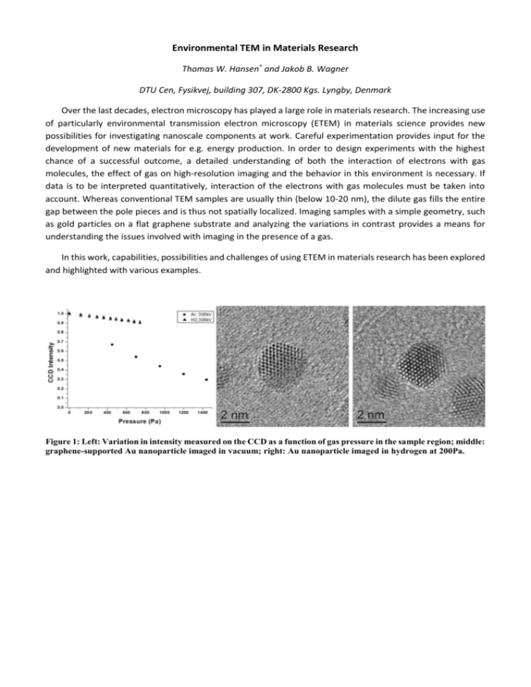
Environmental TEM in Materials Research Thomas W. Hansen* and Jakob B. Wagner DTU Cen, Fysikvej, building 307, DK-2800 Kgs. Lyngby, Denmark Over the last decades, electron microscopy has played a large role in materials research. The increasing use of particularly environmental transmission electron microscopy (ETEM) in materials science provides new possibilities for investigating nanoscale components at work. Careful experimentation provides input for the development of new materials for e.g. energy production. In order to design experiments with the highest chance of a successful outcome, a detailed understanding of both the interaction of electrons with gas molecules, the effect of gas on high-resolution imaging and the behavior in this environment is necessary. If data is to be interpreted quantitatively, interaction of the electrons with gas molecules must be taken into account. Whereas conventional TEM samples are usually thin (below 10-20 nm), the dilute gas fills the entire gap between the pole pieces and is thus not spatially localized. Imaging samples with a simple geometry, such as gold particles on a flat graphene substrate and analyzing the variations in contrast provides a means for understanding the issues involved with imaging in the presence of a gas. In this work, capabilities, possibilities and challenges of using ETEM in materials research has been explored and highlighted with various examples. Figure 1: Left: Variation in intensity measured on the CCD as a function of gas pressure in the sample region; middle: graphene-supported Au nanoparticle imaged in vacuum; right: Au nanoparticle imaged in hydrogen at 200Pa.
