35 GHz bandwidth of Germanium on silicon Metal
advertisement

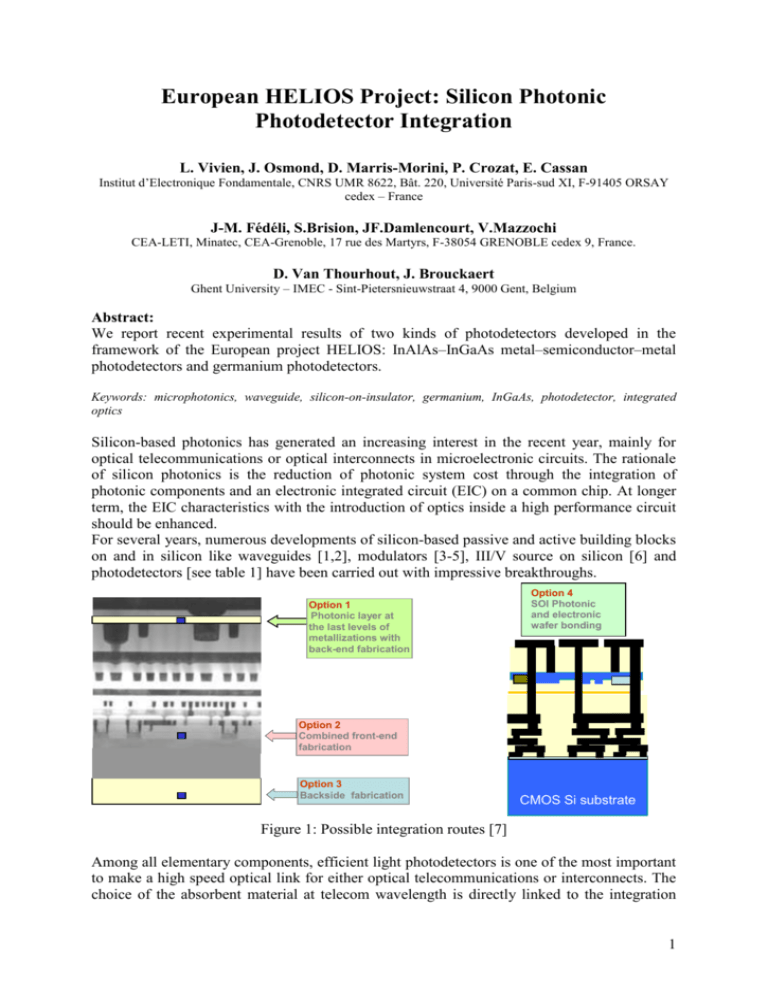
European HELIOS Project: Silicon Photonic Photodetector Integration L. Vivien, J. Osmond, D. Marris-Morini, P. Crozat, E. Cassan Institut d’Electronique Fondamentale, CNRS UMR 8622, Bât. 220, Université Paris-sud XI, F-91405 ORSAY cedex – France J-M. Fédéli, S.Brision, JF.Damlencourt, V.Mazzochi CEA-LETI, Minatec, CEA-Grenoble, 17 rue des Martyrs, F-38054 GRENOBLE cedex 9, France. D. Van Thourhout, J. Brouckaert Ghent University – IMEC - Sint-Pietersnieuwstraat 4, 9000 Gent, Belgium Abstract: We report recent experimental results of two kinds of photodetectors developed in the framework of the European project HELIOS: InAlAs–InGaAs metal–semiconductor–metal photodetectors and germanium photodetectors. Keywords: microphotonics, waveguide, silicon-on-insulator, germanium, InGaAs, photodetector, integrated optics Silicon-based photonics has generated an increasing interest in the recent year, mainly for optical telecommunications or optical interconnects in microelectronic circuits. The rationale of silicon photonics is the reduction of photonic system cost through the integration of photonic components and an electronic integrated circuit (EIC) on a common chip. At longer term, the EIC characteristics with the introduction of optics inside a high performance circuit should be enhanced. For several years, numerous developments of silicon-based passive and active building blocks on and in silicon like waveguides [1,2], modulators [3-5], III/V source on silicon [6] and photodetectors [see table 1] have been carried out with impressive breakthroughs. Option 1 Photonic layer at the last levels of metallizations with back-end fabrication Option 4 SOI Photonic and electronic wafer bonding Option 2 Combined front-end fabrication Option 3 Backside fabrication CMOS Si substrate Figure 1: Possible integration routes [7] Among all elementary components, efficient light photodetectors is one of the most important to make a high speed optical link for either optical telecommunications or interconnects. The choice of the absorbent material at telecom wavelength is directly linked to the integration 1 scheme we choose. Indeed, two kinds of active material can be used to detect light on silicon: germanium which is directly compatible with CMOS technology and III–V compound semiconductors wich can be heterogeneously integrated. Different integration technology options are presented in figure 1. The integration schemes presented in figure 1 require different material strategies for photonic devices, especially for active components. Indeed, in option 1 often called 3D integration or above IC integration, the photonic layer is realized at the metallization levels with back-end of the line technology (BEOL). In this case, all photonic devices are processed at low temperature and efficient III-V material will be used. In the option 2, III-V material can hardly integrated at the level of silicon transistor. While While in other options, either III-V or germanium can be used with a slight preference to consider monolithic integration using germanium instead of III-V components. In the framework of European project Helios, each option will be considered and both III-V and germanium photodetectors integrated in silicon waveguides are studied. Table 1 presents a non-exhaustive state of the art of photodetectors in/on silicon using either III-V materials bonded on Si or germanium on silicon. III-V-on-Si photodetectors Ge-on-Si photodetectors MIT UPS-IEF & LETI INTEL UPS-IEF & LETI PICMOS IMEC INTEL LETI Year 2007 2007 2007 2008 2006 2007 2007 2007 structure PIN MSM PIN PIN PIN MSM PIN PIN Dark current at -1V ~1 µA ~100 µA ~170 nA ~20 nA ~1 nA ~1 nA ~50 nA ~10 nA Responsivity ~1.08 A/W > 1 A/W ~0.9 A/W ~1 A/W ~0.45 A/W ~1 A/W Bandwidth 7.2 GHz 25 GHz 31 GHz 42 GHz 33 GHz - ~0.31 A/W ~0.01 A/W 0.5 GHz - Table 1: Non-exhaustive state of the art germanium and III-V photodetectors on silicon [8-16]. In the framework of the European project HELIOS, compact and efficient InAlAs–InGaAs metal–semiconductor–metal photodetectors and germanium photodetectors integrated on silicon-on-insulator (SOI) waveguides are studied and optimized to achieve data transmission up to 40Gbit/s. dark-current and responsivity at a wavelength of 1.55µm of both III-V and Ge waveguide photodetectors are about few nA and 1 A/W respectively. As an example, we obtained an open eye diagram from a vertical pin Ge-on-Si diode integrated with a rib waveguide, modulated at 40Gb/s, as shown in Fig. 2. 2 Figure 2: (a) Schematic view of vertical pin Ge-on-Si diode integrated in rib waveguide. (b) Open eye diagram at 40Gbit/s. In conclusion, we report recent results of two kinds of photodetectors developed in the framework of the European project HELIOS: InAlAs–InGaAs metal–semiconductor–metal photodetectors and germanium photodetectors. Low dark-current and high responsivity at a wavelength of 1.55µm have been achieved with both photodetectors. Data transmission up to 40 Gbit/s for Ge photodiode has been obtained. Acknowledgement: The research leading to these results has received funding from the European Community's Seventh Framework Programme (FP7/2007-2013) under grant agreement n° 224312 HELIOS. [1] S.Lardenois, D.Pascal, L.Vivien, E.Cassan, S.Laval, R.Orobtchouck, M.Heitzmann, N.Bouzaida, L.Mollard, Low-loss submicrometer silicon-on-insulator rib waveguides and corner mirrors, Opt. Lett. 28, 1150-1152 (2003). [2] W. Bogaerts, D. Taillaert, B. Luyssaert, P. Dumon, J. Van Campenhout, P. Bienstman, D. Van Thourhout, R. Baets, V. Wiaux, and S. Beckx, "Basic structures for photonic integrated circuits in Silicon-on-insulator," Opt. Express 12, 1583-1591 (2004) [3] Delphine Marris-Morini, Laurent Vivien, Jean Marc Fédéli, Eric Cassan, Philippe Lyan, and Suzanne Laval, "Low loss and high speed silicon optical modulator based on a lateral carrier depletion structure," Opt. Express 16, 334-339 (2008) [4] Delphine Marris-Morini, Xavier Le Roux, Laurent Vivien, Eric Cassan, Daniel Pascal, Mathieu Halbwax, Sylvain Maine, Suzanne Laval, Jean Marc Fédéli, and Jean François Damlencourt, "Optical modulation by carrier depletion in a silicon PIN diode," Opt. Express 14, 1083810843 (2006) [5] L. Liao, A. Liu, et al, “40 Gbit/s silicon optical modulator for highspeed applications”, Electronics Letters, 43, (22) (2007). [6] P. Rojo Romeo, J. Van Campenhout, P. Regreny, A. Kazmierczak, C. Seassal, X. Letartre, G. Hollinger, D. Van Thourhout, R. Baets, J. M. Fedeli, and L. Di Cioccio, "Heterogeneous integration of electrically driven microdisk based laser sources for optical interconnects and photonic ICs," Opt. Express 14, 3864-3871 (2006) [7] J.M. Fedeli, L. Di Cioccio, D. Marris-Morini, L. Vivien, R. Orobtchouk, P. Rojo-Romeo, C. Seassal AND F. Mandorlo, Development of silicon photonics devices using microelectronic tools for the integration on top of a CMOS wafer, Advances in Optical Technologies AOT, special issue : "Silicon Photonics", vol. 2008, Article ID 412518, 15 page,( 2008) [8]D. Ahn, C.-yin Hong, J. Liu, W. Giziewicz, M. Beals, L. C. Kimerling, J. Michel, J. Chen and F. X. Kärtner, “ High performance, waveguideintegrated Ge photodetectors,” Opt. express 15 (7), 3916-3921 (2007). [9] L. Vivien, M. Rouvière, J-M. Fédéli, D. Marris-Morini, J-F. Damlencourt, J. Mangeney, P. Crozat, L. El Melhaoui, E. Cassan, X. Le Roux, D. Pascal, and S. Laval, “ High speed and high responsivity germanium photodetector integrated in a Silicon-On-Insulator microwaveguide,” Opt. Express 15 (15), 9843-9848 (2007). [10] T. Yin, R. Cohen, M. M. Morse, G. Sarid, Y. Chetrit, D. Rubin, and M. J. Paniccia, “ 31GHz Ge n-i-p waveguide photodetectors on silicon-on-insulator sunstrate,” Opt. express 15 (21), 13965-13971 (2007). [11] Laurent Vivien, Johann Osmond, Jean-Marc Fédéli, Delphine Marris-Morini, Paul Crozat, Jean-François Damlencourt, Eric Cassan, Y. Lecunff, and Suzanne Laval, "42 GHz p.i.n Germanium photodetector integrated in a silicon-on-insulator waveguide," Opt. Express 17, 6252-6257 (2009) [12] G. Roelkens, D. Van Thourhout, R. Baets, R. Nötzel, and M. Smit, "Laser emission and photodetection in an InP/InGaAsP layer integrated on and coupled to a Silicon-on-Insulator waveguide circuit," Opt. Express 14, 8154-8159 (2006) [13] Joost Brouckaert, Gunther Roelkens, Dries Van Thourhout, and Roel Baets, Compact InAlAs–InGaAs Metal–Semiconductor–Metal Photodetectors Integrated on Silicon-on-Insulator Waveguides, IEEE Phot. Techn. Lett. 19,(2007) [14] Hyundai Park, Alexander W. Fang, Richard Jones, Oded Cohen, Omri Raday, Matthew N. Sysak, Mario J. Paniccia, and John E. Bowers, "A hybrid AlGaInAs-silicon evanescent waveguide photodetector," Opt. Express 15, 6044-6052 (2007) [15] CEA/LETI – Internal report [13] P.R.A. Binetti, X.J.M. Leijtens, T. de Vries, Y.S. Oei, L. Di Cioccio, J.-M. Fedeli, C. Lagahe, J. Van Campenhout, D. Van Thourhout, P.J. van Veldhoven, R. N¨otzel and M.K. Smit, InP/InGaAs Photodetector on SOI Circuitry, Group IV Photonics 2009. 3


