Additional HW problems from CMOS
advertisement
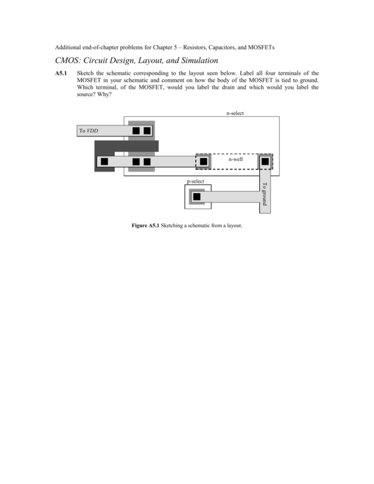
Additional end-of-chapter problems for Chapter 5 – Resistors, Capacitors, and MOSFETs CMOS: Circuit Design, Layout, and Simulation A5.1 Sketch the schematic corresponding to the layout seen below. Label all four terminals of the MOSFET in your schematic and comment on how the body of the MOSFET is tied to ground. Which terminal, of the MOSFET, would you label the drain and which would you label the source? Why? n-select To VDD n-well Figure A5.1 Sketching a schematic from a layout. To ground p-select A5.2 Sketch the corresponding schematic for the following layout. Make sure the body connections of the MOSFETs are clearly seen in your schematic. n-well n-select n-select Out In 15 p-select 2 18 10 p-select To ground Figure A5.2 Sketching a schematic from a layout. A5.3 Using common-centroid techniques lay out matched 10k resistors using unsilicided polysilicon. Use a unit-cell size of 2 kΩ. Final connection to the resistors should be made on metal2. A5.4 Write a short tutorial covering lateral diffusion and oxide encroachment. Use both layouts and cross-sectional views to help with the clarity of your tutorial. A5.5 Design a test structure to measure overlap capacitance for an NMOS device. Lay the test structures out with probe pads (not bond pads). Comment on how the testing is performed. Use SPICE to simulate the tests using the device W/L you selected. Compare the results to your hand calculations. Note this is a very practical problem that requires a simple solution. Make sure it is very clear you demonstrate, through your clear homework solutions, that you know what you are doing. A5.6 Using a schematic capture program draw the schematic of the resistive divider in Fig. 5.4b on page 109. Use a unit resistor size of 10k. Simulate the operation of the circuit. A5.7 Lay out a poly-poly 1 pF capacitor. Comment on how you size the (drawn) layout (use a lambda is 0.3 µm). A5.8 Sketch the CV curve for the capacitance on the drain terminal of an NMOS device (see below) against increasing drain voltage. Sketch the cross sectional view showing how the depletion width changes with increasing drain voltage for both the bottom and sidewall components. D Figure A5.8 How the capacitance on the drain of the MOSFET changes with applied potential A5.9 Layout a 1000/2 NMOS device in as square an area as possible (remember a MOSFET has four terminals). A5.10 Suppose the bottom plate parasitic in the poly1-poly2 capacitor seen below is 25% of the desired capacitance value (here 1 pF). Sketch the equivalent schematic of the circuit. If the resistor is large so its effects can be neglected estimate the output voltage if the input voltage changes from 0 to VDD. If the resistor value is 10k and an AC voltage is applied to the input estimate the frequency where the output AC voltage is half of the AC input voltage. 1 pF Input Output Figure A5.10 Estimating the effects of the parasitic bottom plate capacitance.
