Self aligned depletion type optical modulator with large
advertisement
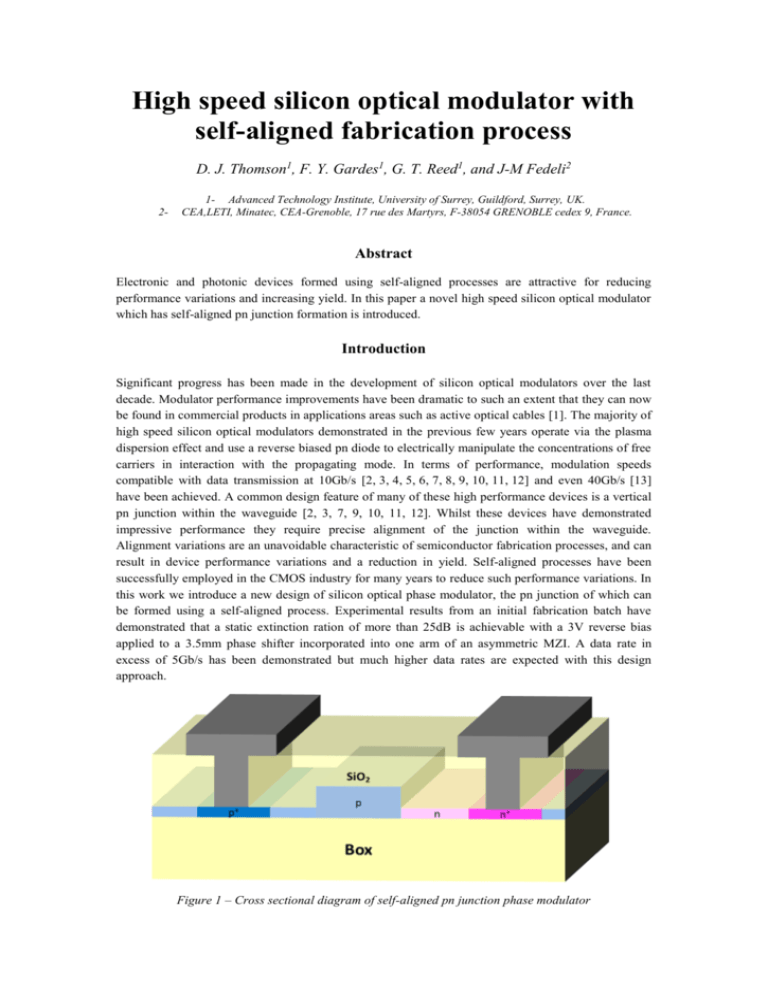
High speed silicon optical modulator with self-aligned fabrication process D. J. Thomson1, F. Y. Gardes1, G. T. Reed1, and J-M Fedeli2 2- 1- Advanced Technology Institute, University of Surrey, Guildford, Surrey, UK. CEA,LETI, Minatec, CEA-Grenoble, 17 rue des Martyrs, F-38054 GRENOBLE cedex 9, France. Abstract Electronic and photonic devices formed using self-aligned processes are attractive for reducing performance variations and increasing yield. In this paper a novel high speed silicon optical modulator which has self-aligned pn junction formation is introduced. Introduction Significant progress has been made in the development of silicon optical modulators over the last decade. Modulator performance improvements have been dramatic to such an extent that they can now be found in commercial products in applications areas such as active optical cables [1]. The majority of high speed silicon optical modulators demonstrated in the previous few years operate via the plasma dispersion effect and use a reverse biased pn diode to electrically manipulate the concentrations of free carriers in interaction with the propagating mode. In terms of performance, modulation speeds compatible with data transmission at 10Gb/s [2, 3, 4, 5, 6, 7, 8, 9, 10, 11, 12] and even 40Gb/s [13] have been achieved. A common design feature of many of these high performance devices is a vertical pn junction within the waveguide [2, 3, 7, 9, 10, 11, 12]. Whilst these devices have demonstrated impressive performance they require precise alignment of the junction within the waveguide. Alignment variations are an unavoidable characteristic of semiconductor fabrication processes, and can result in device performance variations and a reduction in yield. Self-aligned processes have been successfully employed in the CMOS industry for many years to reduce such performance variations. In this work we introduce a new design of silicon optical phase modulator, the pn junction of which can be formed using a self-aligned process. Experimental results from an initial fabrication batch have demonstrated that a static extinction ration of more than 25dB is achievable with a 3V reverse bias applied to a 3.5mm phase shifter incorporated into one arm of an asymmetric MZI. A data rate in excess of 5Gb/s has been demonstrated but much higher data rates are expected with this design approach. Figure 1 – Cross sectional diagram of self-aligned pn junction phase modulator Device design and fabrication A cross-sectional diagram of the device is shown in figure 1. The phase modulators are formed in waveguides with dimensions of 220nm in height, 450nm in width and 50nm in slab height. The rib region is doped lightly p type and an n type region is positioned at the edge of the waveguide. The doping concentrations of these regions are then asymmetric, such that the majority of the depletion occurs in the waveguide, in the p-type material. To ensure resistive contact to the electrodes, highly doped regions are formed below the contacts, positioned approximately 675nm away from the waveguide edge such that excessive optical loss is not caused. The phase modulators are incorporated into Mach Zehnder interferometers (MZI) to translate the phase modulation into intensity modulation. Compact multimode interference (MMI) structures are used to perform the splitting and combining function in the MZI. Phase modulators are placed into both arms of the MZI to balance the optical power and therefore permit a large static extinction ratio. Coplanar waveguide (CPW) electrodes are used to drive the modulator at high speed. The CPWs were designed to have a characteristic impedance of 50 ohms, taking into account the effects of the diode capacitance. Device fabrication was performed in the cleanroom facilities at CEA-LETI. Devices are fabricated in 220nm overlayer SOI from SOITEC, which has a 2um thick buried oxide layer. Firstly the active regions are implanted with boron to make them lightly p type. The waveguide patterns are then formed in an SiO2 layer which is deposited onto the surface. This layer firstly acts as a hard mask through which to etch the optical waveguides. The remaining SiO2 hard mask is then used together with a resist defined implant window to form the n type region at the side of the rib. Since one edge of the phosphorus implanted region butts up against the side of the waveguide, the edge of the resist implant window can be roughly aligned anywhere on top of the waveguide. This crucial step in the process is therefore self-aligned. The remaining process steps used to form the highly doped regions and contacts are performed using standard CMOS processes. In future device iterations self alignment of more steps will also be possible making the design even more robust against typical fabrication tolerances. Experimental results Asymmetrical MZIs are used to allow convenient analysis of the DC modulation performance of the fabricated devices. A tuneable laser source with a wavelength range centred on 1550nm is coupled into and out of the devices using out of plane grating couplers. An optical detector is used to measure the output optical power from the device. Wavelength scans are then performed with different reverse bias signals applied to the diode, which cause different amounts of wavelength shift as shown in the results of figure 2 which were obtained from a 3.5mm long phase shifter. Normalised output (dB) 0 -10 -20 -30 -40 -50 0V -3V -6V -9V 1546 1548 1550 1552 1554 Wavelength (nm) Figure 2 - Modulator normalised spectral response A static extinction ratio of almost 40dB is achieved for the MZI structure. This allows for large DC extinction ratios to be achieved with modest phase shifts, for example, if operating at the minima close to 1556.4nm on the 0V curve, a DC extinction ratio of approximately 25dB can be achieved with a DC voltage of just 3V. The modulation efficiency of the device from figure 2 can be evaluated as 8V.cm with an optical loss of approximately 7dB. Devices from other positions on the wafer have reported efficiencies as little a 6V.cm. The performance of the above device at high speed has been analysed using a PRBS signal generator of variable output rate and driver amplifier. As can be seen in figure 3, the optical eye is open at 1.5Gb/s with approximately a 3dB extinction ratio. An open eye is also obtainable at faster data rates (4Gb/s also shown in figure 3), up to more than 5Gb/s. The results from the modulator devices and test structures of this initial batch have been used to optimise the design and fabrication process for a second run, from which much enhanced results are expected. 1.5Gb/s 4Gb/s Figure 3 – Data transmission at 1.5Gb/s (left) and 4Gb/s (right) Conclusion A novel high speed silicon optical modulator has been reported which allows for a self aligned process to be used to form the pn junction. Self aligned processes can allow for the fabrication of future silicon photonic devices with reduced performance variations. Experimental results from an initial fabrication batch have demonstrated promising results, achieving a DC extinction ratio of approximately 25dB with just a 3V reverse bias on a 3.5mm phase shifter. Open eye diagrams have been observed at up to 5Gb/s. Developments made to the design and processing are expected to yield much enhanced results from the devices currently being fabricated. Acknowledgements The research leading to these results has been performed within the European Community's Seventh Framework Programme (FP7/2007-2013) under grant agreement n° 224312 HELIOS. References [1] - D. D’Andrea in Proc. OFC, 2009, San Diego, 2009. [2] - F. Y. Gardes et al. Opt. Express, Vol. 17, pp. 21986-21991, 2009. [3] - P. Dong et al. Opt. Express, Vol. 17, pp. 22484-22490, 2009. [4] - J.-B. You et al.Opt. Express, Vol. 16, pp. 18340-18344, 2008. [5] - D. Marris-Morini et al. Optics Express, Vol. 14, pp. 10838-10843, 2006. [6] - C. Gunn, Micro, IEEE, Vol. 26, pp. 58-66, 2006. [7] - J. W. Park et al. Opt. Express, Vol. 17, pp. 15520-15524, 2009. [8] - A Narasimha et al., in Proc. OFC, 22-25 March, San Diego, USA 2010. [9] - L. Tsung-Yang et al. IEEE Journal of Selected Topics in Quantum Electronics, Vol. 16, pp. 307-315, 2010. [10] – D. M. Gill et al. IEEE Photonics Technology Letters, Vol. 21, No. 4, pp. 200-2, 15 Feb. 2009 [11] - S. J. Spector et al. 2008 Conference on Lasers and Electro-Optics (CLEO), May 2008 [12] - N.-N. Feng et al. Opt. Express, Vol. 18, No. 8, pp. 7994-7799, 12 April 2010 [13] – L. Liao et al., Electronics Letters, Vol. 43, No. 22, pp. 1196-7, 25 Oct. 2007
