Required skills: basic knowledge of crystallography and X
advertisement
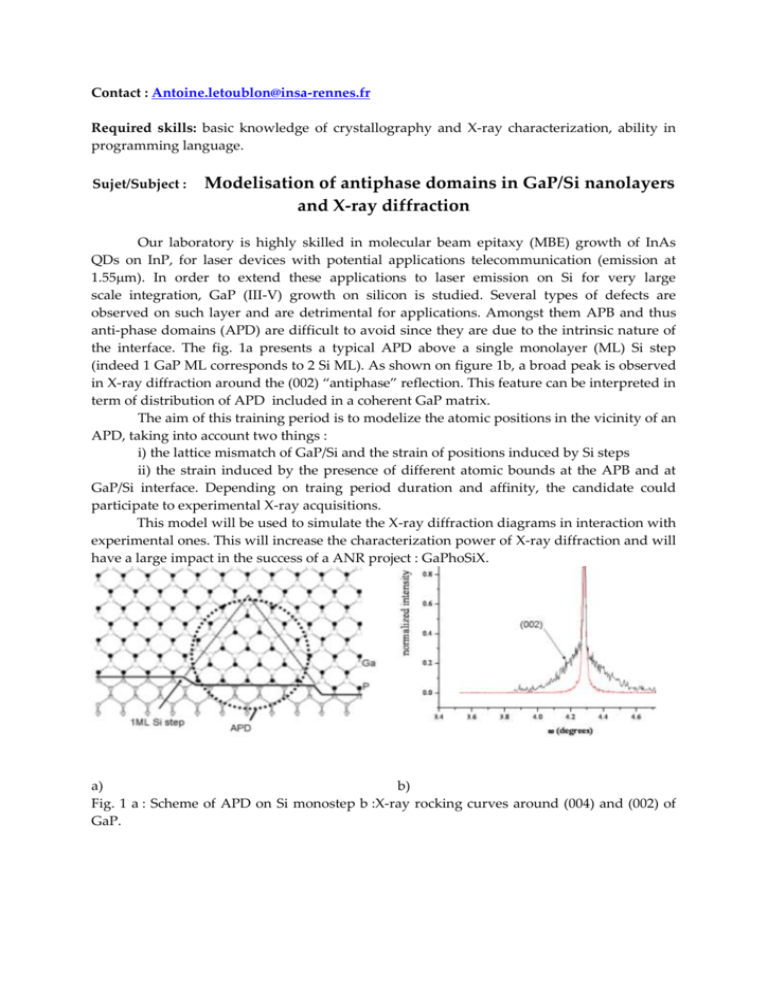
Contact : Antoine.letoublon@insa-rennes.fr Required skills: basic knowledge of crystallography and X-ray characterization, ability in programming language. Sujet/Subject : Modelisation of antiphase domains in GaP/Si nanolayers and X-ray diffraction Our laboratory is highly skilled in molecular beam epitaxy (MBE) growth of InAs QDs on InP, for laser devices with potential applications telecommunication (emission at 1.55m). In order to extend these applications to laser emission on Si for very large scale integration, GaP (III-V) growth on silicon is studied. Several types of defects are observed on such layer and are detrimental for applications. Amongst them APB and thus anti-phase domains (APD) are difficult to avoid since they are due to the intrinsic nature of the interface. The fig. 1a presents a typical APD above a single monolayer (ML) Si step (indeed 1 GaP ML corresponds to 2 Si ML). As shown on figure 1b, a broad peak is observed in X-ray diffraction around the (002) “antiphase” reflection. This feature can be interpreted in term of distribution of APD included in a coherent GaP matrix. The aim of this training period is to modelize the atomic positions in the vicinity of an APD, taking into account two things : i) the lattice mismatch of GaP/Si and the strain of positions induced by Si steps ii) the strain induced by the presence of different atomic bounds at the APB and at GaP/Si interface. Depending on traing period duration and affinity, the candidate could participate to experimental X-ray acquisitions. This model will be used to simulate the X-ray diffraction diagrams in interaction with experimental ones. This will increase the characterization power of X-ray diffraction and will have a large impact in the success of a ANR project : GaPhoSiX. a) b) Fig. 1 a : Scheme of APD on Si monostep b :X-ray rocking curves around (004) and (002) of GaP.
