Preparation of Papers in a Two-Column Format for the 21st Annual
Modeling of Haptic Sensing of Nanolithography with an
Atomic Force Microscope
*
Wen J. Li L. M. Fok and Y. H. Liu
Robotics Laboratory
The Chinese University of Hong Kong
Center for Micro and Nano Systems
The Chinese University of Hong Kong lmfok@acae.cuhk.edu.hk, yhliu@acae.cuhk.edu.hk wen@acae.cuhk.edu.hk
Abstract -
This paper describes a virtual reality interface between human and the Atomic Force Microscope (AFM), which allows the operator to perform nanomanipulation with an AFM tip in the virtual reality environment with haptic feedback. During operation, the tip-sample interaction forces and intermolecular forces between the tip and surface are modeled based on Lennard-Jones potential and JKR theory, respectively. Our objective is to provide a 3D virtual reality interface capable of displaying topography of surface for the users and allow them to predict the results for the manipulation.
Index Terms -
Atomic Force Microscope, Haptic Interface,
Nanomanipulation, Virtual Reality.
I.
I NTRODUCTION surface will give rise to a deflection in the opposite direction, which indicates that the tip is still in contact with the surface. At a certain point, the tip pulls out from the surface and the cantilever is still bending downward under the influence of the tip-sample force. When it is retracted farther from the surface, it returns to its original position.
The atomic force microscope (AFM) is a system that is used to determine roughness, grain size, or features of surface at atomic level [1] – [3]. It can profile samples in real, three-dimensional space with vertical resolutions to 0.1 nm. Because the AFM does not rely on the presence of a tunneling current, a wide range of materials can be used for investigation including semiconductors, non-conducting surfaces, insulators, and biological samples.
The AFM makes use of a probe that has a microfabricated tip mounted on an elastic cantilever to record the attractive and repulsive forces between the tip and the surface. During contact mode operation, the tip is slowly scanned across the surface and is gently in contact with it.
The lateral and vertical movements of the tip or sample are controlled by piezoelectric scanners and a feedback loop that produce voltage differences proportional to the movement.
The interatomic forces between the atoms on the surface of
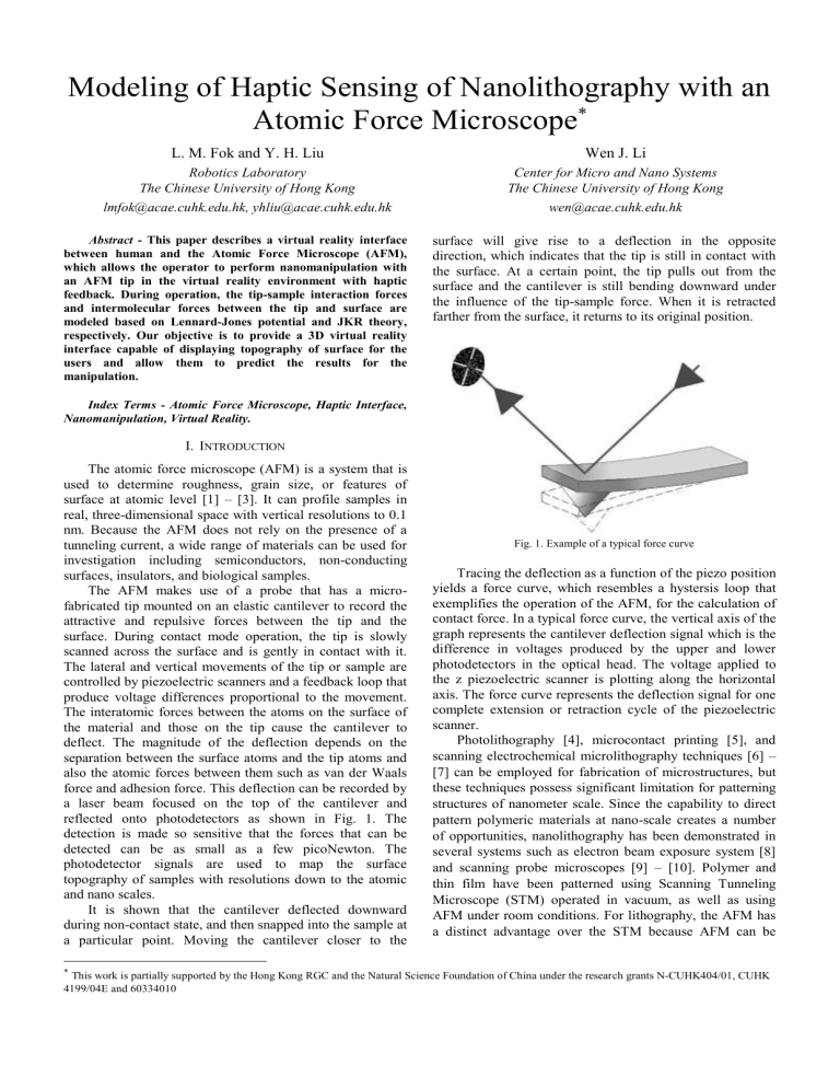
Fig. 1. Example of a typical force curve
Tracing the deflection as a function of the piezo position yields a force curve, which resembles a hystersis loop that exemplifies the operation of the AFM, for the calculation of contact force. In a typical force curve, the vertical axis of the graph represents the cantilever deflection signal which is the difference in voltages produced by the upper and lower photodetectors in the optical head. The voltage applied to the z piezoelectric scanner is plotting along the horizontal axis. The force curve represents the deflection signal for one complete extension or retraction cycle of the piezoelectric scanner.
Photolithography [4], microcontact printing [5], and the material and those on the tip cause the cantilever to deflect. The magnitude of the deflection depends on the separation between the surface atoms and the tip atoms and also the atomic forces between them such as van der Waals force and adhesion force. This deflection can be recorded by a laser beam focused on the top of the cantilever and scanning electrochemical microlithography techniques [6] –
[7] can be employed for fabrication of microstructures, but these techniques possess significant limitation for patterning structures of nanometer scale. Since the capability to direct reflected onto photodetectors as shown in Fig. 1. The detection is made so sensitive that the forces that can be detected can be as small as a few picoNewton. The photodetector signals are used to map the surface topography of samples with resolutions down to the atomic and nano scales.
It is shown that the cantilever deflected downward during non-contact state, and then snapped into the sample at a particular point. Moving the cantilever closer to the pattern polymeric materials at nano-scale creates a number of opportunities, nanolithography has been demonstrated in several systems such as electron beam exposure system [8] and scanning probe microscopes [9] – [10]. Polymer and thin film have been patterned using Scanning Tunneling
Microscope (STM) operated in vacuum, as well as using
AFM under room conditions. For lithography, the AFM has a distinct advantage over the STM because AFM can be
*
This work is partially supported by the Hong Kong RGC and the Natural Science Foundation of China under the research grants N-CUHK404/01, CUHK
4199/04E and 60334010
used for insulating as well as conducting materials. And patterning by the AFM tip is a non-damaging process with higher precision of alignment and narrower width of lithography than those obtained by the use of photon, electron and scanning probe lithography.
In contact mode, the probe is in contact with the surface and the AFM uses various forces that occur when two objects are brought within nanometers of each other. By indenting the tip onto the sample, patterning on a length scale below 10 nm can be realized such as modification of polymer and direct patterning. Varying the magnitude of the applied load can perform either deep scratching or frictionless sliding. There are two ways to vary the applied force which are either by setting the displacement of piezoelectric scanners on defined distance along z axis or tuning the trigger threshold value.
However, AFM-based manipulation is usually not instinctive to the user and requires a high degree of training.
With the aid of a force feedback device, direct positioning of the AFM tip with nanometer precision becomes possible. In
[11] – [12], a direct manipulation system with force feedback and 3D virtual reality graphics display are utilized for nanomanipulation. However, direct manipulation is usually slow and imprecise, results also cannot be estimated.
Later on, closed-loop task-oriented autonomous control [13] was developed to avoid problems. This system is limited by executing only the given tasks without user intervention.
Yet, the automatic control in nanoworld is still challenging due to the complexity of the nanoscale dynamics.
This paper is focused mainly on developing a nanomanipulation system with a haptic interface using a force feedback joystick and a 3D virtual reality graphic display. The force feedback joystick implemented in the system was a Wingman Force of Logitech with high sensitivity performance, which serves as a haptic interface which provides the users with the sensation of tip-sample interactions. The graphical user interface was developed from the topography data fed from the AFM, which displays the surface topography and the position of the AFM tip on the sample. Users are allowed to control the whole system by the joystick and switch between navigation and manipulation mode. Within the non-contact regime, the tipsample interaction force is modeled by the Lennard-Jones potential [14] and soon after they are being in contact, the adhesion force is simulated based on the Johnson-Kendall-
Roberts (JKR) theory [15]. The topography data is scaled to perform the appropriate response on the force feedback joystick and users feel a force proportional to the height of the sample point interacting with the AFM tip.
II.
M ODELING O F I NTERATOMIC F ORCES
The interaction between the tip and sample of an atomic force microscope consists of a variety of forces such as van da Waals, electric, and magnetic forces for the non-contact regime and adhesion, and capillary forces for the contact regime. In which, van da Waals and adhesion forces are being most significant for the calculation for the interatomic forces. The van da Waals force is worked out from the
Lennard-Jones potential and the adhesion force is evaluated from the JKR theory.
A. Indentation and Adhesion Forces
The tip and sample are represented as two spheres and define the effective tip-sample radius of curvature as
R
R
R
1
1
R
2
R
2
.
(1) where R and
1
R are the radius of curvature of the AFM tip
2 and sample, respectively.
The surface energy,
required to separate two flat surfaces from contact to infinity.
H
24
D
0
2
W
1 , 2
2
(2) where
(
/ 2 .
5
H is the Hamaker’s constant,
),
0 .
4125 nm
D
0
is the typical interatomic distance, and W
1 , 2
is the work of adhesion.
According to the JKR theory, the elastic modules of the two spheres are defined as
1
1
E
1
1
2 (3)
And
2
1
E
2
2
2 (4) where E i
is the Young’s modulus, and ratio. The effective elastic modulus,
i
is the Poisson’s
, is then expressed as
1
2
(5)
The tip-sample contact forces as a function of the contact radius is
F
Kr 3
R
2 Kqr 3
R
,
(6) where K
4
3
, and
The indentation, q
3
RW
1 , 2
. d in
, as a function of the applied force is d in
r
2
3 R
2 F
3 rK
.
(7)
B. Lennard-Jones Forces
Denote the initial position of the AFM cantilever by u and the displacement of the tip by s . The deflection of the cantilever, d , is described as d = s – u . The deflection of the cantilever is expressed as a function of the piezo displacement. The Lennard-Jones potential, W , is used for modeling of interactive forces in non-contact regime and is given by
W
HR
1
6
1
210
s
7
s
.
(8)
The Lennard-Jones force, F
L
, is obtained from the potential by taking the negative of its derivative with respect to s.
F
L
HR
1
30 s 6
180 s 8
6
.
(9)
C. Snap-in and Pull-out Points
The deflection of the cantilever as a function of the piezo displacement is expressed as d
F
L k
,
(10) where k is the spring constant of the cantilever.
The tip jumps to contact with the surface (snap-in) or pulls out of the surface (pull-out) when the derivative of the force equals to the spring constant. The values of snap-in and pullout point are obtained by solving dF ds
L
k .
(12)
III.
E XPERIMENTAL P ROCEDURES
In this experiment, the AFM is employed as a tool for nanolithography by controlled tip motion on various material surfaces. Nanolithography may be used to investigate various material properties and this could be conducted within the area bounded by the maximum scan size. The deflection of the cantilever accomplishes as a measure of the force.
Generally, the process includes the following steps:
1.
Obtain an image by contact or tapping mode scanning
2.
Determine the lithography location
3.
Adjust the sample or offset to position
4.
Verify that the sample is leveled in both x-axis and yaxis
5.
Force the tip along z-axis towards the surface at specified rate until the required cantilever deflection is reached
6.
Perform lithography by moving the tip laterally by a prescribed distance and direction
7.
Lift up the tip to its initial z position
8.
Repeat imaging of the surface
Trigger Threshold deflection at the surface contact point, which locates at the flat portion of the force plot where the force is zero.
The cantilever sensitivity is the cantilever deflection signal versus the voltage applied to the z piezoelectric scanner determined from the slope of the force plot. The sensitivity of the cantilever must be verified in order to calculate the force applied to the sample during indentation.
Once the sensitivity is being known, the force, indentation is determined from Hooke’s Law,
F z
k
x
k
V t
.
s
F z
, of
(13) where x is the cantilever deflection in nm, V t
is the trigger threshold voltage, and s is the cantilever sensitivity in nm/V.
The cantilever deflection is determined from the cantilever sensitivity and the maximum deflection used for the indentation.
IV.
R ESULTS AND D ISCUSSIONS
The graphical interface was developed based on the topographic data obtained from the AFM. The 3D surface was generated according to the height data and users are allowed to perform navigation of the surface in a virtual reality environment as shown in Fig. 3(a). Besides, users can execute lithography on the surface in manipulation mode as shown in Fig. 3(b). Fig. 3(c) and 3(d) show the surface before and after simulation, respectively. The depth of indentation is estimated by the JKR theory.
TABLE I
SETTING OF PARAMETERS FOR SIMULATION
Parameters Value
Tip radius 30 nm
Sample radius
Young’s modulus of Au
Young’s modulus of Polymer
100 nm
0 .
08
10 1 2 N / m 2
0 .
001
10 1 2 N / m 2
Poisson ratio of Au
Poisson ratio of Polymer
Hamaker’s constant of Au
Hamaker’s constant of Polymer
0.42
0.3
45 .
5
10
2 0 J
6 .
2
10
2 0 J
Fig. 2. Example of force plot
In each operation, a force plot is recorded. The Trigger threshold is the value of the cantilever deflection, as measured by the photodetector, desired for the indentation or lithography. It defines the maximum force applied to the sample corresponding to the upper leftmost point on the force plot as shown in Fig. 2. During the process, the tip is pushed into the surface until the cantilever deflection equals to the trigger threshold. Then the tip is moved laterally in a prescribed direction in order to perform lithography. The cantilever deflection is measured relative to the value of the
(a)
(b)
(c) values of snap-in and pull-out were 2.13 nm and 12.79 nm , respectively. The results illustrated that higher attractive force were produced between the gold-coated tip and the gold surface than that for the polymer surface.
In the manipulation mode, the contact radius between the tip and sample surface is being monitored and it is used for the computation of the applied force by the user. Prior to the simulation, users are allowed to modify the setting of parameters. The depth of indentation is estimated by the applied force of the user. According to the parameters defined in Table 1, the depth of lithography with applied force of 1.35
N was 33 nm . Fig. 4 illustrates the depth of indentation increased with increasing applied load. In comparison, the gold film showed higher resistance to indentation than the polymer thin film since the depth of indentation was only 2.7 nm for a force of 1.35
N .
-10
-15
0
-5
0
-20
-25
-30
-35
200
Applied Force (nN)
400 600 800 1000 1200 1400
Polymer Surface Gold Surface
Fig. 4. The depth of indentation as a function of the applied force
(d)
Fig. 3 Screen shots of virtual reality graphical display
When the distance between the tip position and the sample surface is below the range of 100 nm , the van da
Waals force is being simulated and it is used to determine the snap-in and pull-out position. As an example, when a silicon cantilever is scanning over a gold surface and a polymer surface, the interatomic forces are simulated based on the parameter settings in Table 1. During the scanning of a gold surface with a gold-coated silicon nitrate cantilever, the calculated values of snap-in and pull-out were 2.98 nm and 34.14 nm , respectively. For a polymer surface, the
Fig 5. Atomic Force Microscope employed for experiment
The AFM used for this study is the Nanoscope III,
Digital Instrument with a silicon nitrate cantilever of tip radius 30 nm , and stiffness of 0.6 N/m . All measurements were performed in an ambient environment. The Parylene thin film was produced by deposition of Parylene C on Si
(100) wafers, which was about 0.3
m thick. Samples were scanned orthogonal to the long axis of the cantilever with average load 1.5
N to generate scratches. Observations of
the sample surface before and after the scratch tests were done by scanning parallel to the long axis of the cantilever with loads of 0.2
N as the parallel scans enable minimum wear of the sample surface. Scratch test consisted of generating scratches in a replicate mode at a given load for 2,
3 and 4 cycles over a scan length of 5
m at 5
m/s .
Fig. 6 and Fig. 7 show the 3D image of the three scratches on the Parylene thin film and 2D sections of the lithography, respectively. The first scratch on the right was made by 2 cycles of scanning, followed by 3 cycles in the middle and 4 cycles on the left.
4 cycles
3 cycles
2 cycles
Fig. 6. 3D images of lithography Parlyene C surface
4 cycles 3 cycles 2 cycles
45
35
25
2 3
Number of cycles
(a)
4
250
200
150
100
2 3 4
Number of cycles
(b)
Fig. 8. (a) Scratch depths as a function of number of cycles
(b) Scratch widths as a function of number of cycles
The depths and widths of scratches were plotted against number of cycles in Fig 8(a) and 8(b), respectively. With constant applied load, the depth and width increase almost linearly with increasing number of cycles. This suggested that the material was removed layer by layer during the test.
Fig. 7. 2D topographic image and 2D sections after lithography
(a)
(b)
(c)
5.6 nm
15.5 nm
25.1 nm
(d)
Fig. 9. Lithography of a channel between gold electrodes on silicon surface
This technique was applied to fabrication of nanochannel between gold electrodes on silicon substrate as shown in Fig. 9. Fig. 9(a) and Fig. 9(b) show the topography of the device before and after nanolithography, respectively.
Fig. 9(c) and Fig 9(d) show the image and 2D section of the channel, where the width and the maximum depth are about
800 nm and 25.5 nm , respectively. The depth of the channel varied with the number of cycle of scratch. The AFM based nanolithography guarantees for precision in localization.
V.
C ONCLUSIONS
This paper describes nanomanipulation system integrated with an AFM provided with a haptic interface and a 3D virtual reality display, which allows the user to act on and feel the nanoworld phenomena through navigation and manipulation. The Lennard-Jones potential is employed to model of tip-sample interaction forces when the AFM tip and material surface are in contact. Indentation and adhesion forces are modeled from JKR theory for contact regime. The motion behaviors of the AFM cantilever and relations between the applied force and depth of indentation have been analyzed. The experimental results provide insight into the mechanics of an AFM-based nanolithography. Models for friction and capillary forces will be implemented in the future so that manipulation by the use of force feeling will become more accurate and predictable.
Nanolithography with contact mode imaging technique has been shown to be a powerful tool. Scratches of various depths and widths were produced and controlled by the number of cycles. An advantage of using AFM for nanolithography over other instruments is that precise localization could be performed based on the high resolution image obtained.
R EFERENCES
[1] J. Mou, D. M. Czajkowsky, S. J. Sheng, R. Ho, and Z. Shao, “High resolution surface structure of E. coli GroeS Oligomer by Atomic
Force Microscopy,” FEBS Letters , vol. 381, pp.161 – 164, 1996.
[2] Y. E. Strausser, M. Schroth, and J. J. Sweeney, “Characterization of the low-pressure chemical vapor deposition grown rugged polysilicon surface using atomic force microscopy,” J. Vas. Sci. Technol. A , vol.
15, pp. 1007, 1997.
[3] W. Fritzsche, L. Takac, and E. Henderson, “Application of atomic force microscopy to visualization of DNA, chromatin, and chromosomes,” Critical Reviews in Eukaryotic Gene Expression , vol.
7, pp. 231 – 240, 1997.
[4] S. Roth, L. Dellmann, G. A. Racine, and N. F. de Rooij, “High aspect ratio UV photolithography for electroplated structures,” J.
Micromech. Mecroeng.
, vol. 9, pp. 105 – 108, 1999.
[5] E. Kim, G. M. Whitesides, M. B. Freiler, M. Levy, J. L. Lin, and R.
M. Osgood Jr., “Fabrication of micrometer-scale structures on GaAs and GaAs/AlGaAs quantum well material using microcontact printing,” Nanotechnology , vol. 7, pp. 266 – 269, 1996.
[6] H. Ohji, P. T. J. Gennissen, P. J. French, and K. Tsutsumi,
“Fabrication of a beam-mass structure using single-step electrochemical etching for micro structures (SEEMS),” J.
Micromech. Microeng.
, vol. 10, pp. 440 – 444, 2000.
[7] R. A. Said, “Microfabrication by localized electrochemical deposition: experimental investigation and theoretical modeling,”
Nanotechnology , vol. 15, pp. 867, 2004.
[8] H. Iwasaki, T. Yoshinobu, and K. Sudoh, “Nanolithography on
SiO
2
/Si with a scanning tunneling microscope,” Nanotechnology , vol.
14, pp. 55 - 62, 2003.
[9] A. Majumdar, P. I. Oden, J. P. Carrejo, L. A. Nagahara, J. J. Graham, and J. Alexander, “Nanometer-scale lithography using the atomic force microscope,” Applied Physics Letters , vol. 61, pp. 2293-2295,
1992.
[10] C. K. Hyon, S. C. Choi, S. H. Song, S. W. Hwang, M. H. Son, D.
Ahn, Y. J. Park, and E. K. Kim, “Application of atomic-forcemicroscope direct patterning to selective positioning of InAs quantum dots on GaAs,” Applied Physics Letters , vol. 77, pp. 2607 – 2609,
2000.
[11] M. Falvo, R. Superfine, S. Washburn, M. Finch, R. M. Taylor, V. L.
Chi, and F. P. Brooks Jr.., “The nanomanipulator: A teleoperator for manipulating materials at the nanomerter scale,” Proc. of Int. Symp.
On Science and Technology of Atomically Engineered Materials , pp.
579 – 586, 1996.
[12] M. Sitti, and H. Hashimoto, “Tele-nanorobotics using atomic force microscope as a robot and sensor,” Advanced Robotics Journal , vol.
13, no. 4, pp. 417 – 436, 1999.
[13] M. Sitti, and H. Hashimoto, “Two-dimensional fine particle positioning under optical microscope using a piezoresistive cantilever as a manipulator,” Journal of Micromechatronics , vol. 1, no. 1, pp.
25 – 48, 2000.
[14] P. L. Huyskens, W. A. P. Luck, and T. Z. Huyskens, Intermolecular
Force, An Introduction to Modern Methods and Results , Spring-
Verlag, Berlin, Heidelbery, 1991.
[15] J. Israelachvili, Intermolecular and Surface Force , Academic Press,
2 nd edition, 1991.
