7 The Time Dimension II
advertisement
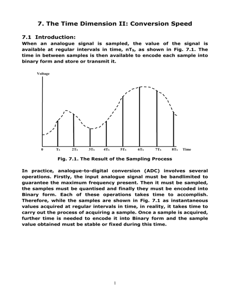
7. The Time Dimension II: Conversion Speed 7.1 Introduction: When an analogue signal is sampled, the value of the signal is available at regular intervals in time, nTS, as shown in Fig. 7.1. The time in between samples is then available to encode each sample into binary form and store or transmit it. Voltage 0 TS 2TS 3TS 4TS 5TS 6TS 7TS 8TS Time Fig. 7.1. The Result of the Sampling Process In practice, analogue-to-digital conversion (ADC) involves several operations. Firstly, the input analogue signal must be bandlimited to guarantee the maximum frequency present. Then it must be sampled, the samples must be quantised and finally they must be encoded into Binary form. Each of these operations takes time to accomplish. Therefore, while the samples are shown in Fig. 7.1 as instantaneous values acquired at regular intervals in time, in reality, it takes time to carry out the process of acquiring a sample. Once a sample is acquired, further time is needed to encode it into Binary form and the sample value obtained must be stable or fixed during this time. 1 7.2 The Sample and Hold Process: This operation is normally carried out by a Sample-and-Hold Amplifier as shown in Fig. 7.2. This is essentially a buffer amplifier with unity gain but which has a transistor switch, T, on the input and a capacitance, C, which can hold the sampled voltage between samples with negligible discharge. When a HI logic level is applied to the control input of the transistor it acts like a closed switch having a low but finite value of resistance and current flows from the input source through the transistor and charges up the capacitor. When a LO logic level is applied to the control input of the transistor, it operates like an open switch so that the charging path is broken and the capacitor remains at the potential reached. sample / hold R→∞ T input voltage Fig 7.2 buffer amplifier output voltage C Simplified Schematic of a Sample-and-Hold Amplifier 2 The amplifier has therefore two modes of operation: the ‘Sample’ mode and the ‘Hold’ mode, which can be seen in Fig. 7.3. In the sample mode the switch closes to allow the output voltage to charge up to and then follow the input voltage, thus acquiring a sample of the input signal. Once it has reached the value of the input signal it will continue to track the input voltage until it is switched to the hold mode. Then in the hold mode it ceases to track the input signal and holds the output voltage at the value of the input signal which prevailed at the instant the amplifier was switched from the sample to the hold mode. output signal V input signal V sample hold sample hold sample hold sample t Fig. 7.3 Waveforms Showing Operation of Sample-and-Hold Amplifier 3 During sampling, when the transistor switch is closed, it has a finite ON resistance, R. Thus the equivalent electrical circuit can be considered as a series Resistor-Capacitor or R-C charging circuit as shown in Fig. 7.4. The product of the resitance, R and the capacitance, C is referred to as the Time Constant of the circuit and characterises the exponential waveform representing the voltage accumulated on the capacitor, C, as a function of time. The time contant of the charging circuit must be small enough to allow the capacitor to reach the maximum input signal voltage, starting from zero if necessary. It can be shown theoretically that it takes a time approximately equal to five times the time constant, CR, of the circuit to reach its final charging value as indicated in Fig. 7.4. R input voltage C sampled voltage V maximum input signal voltage Vin max sampled voltage (time constant CR) 0 Tsample ≈ 5CR Fig. 7.4 t Operation of a Capacitor-Resistor Charging Circuit This means that the time it takes to obtain a sample, TSAMPLE , can be closely approximated as: TSAMPLE 5CR 4 7.3 Conversion Rate: In the hold mode the ouput of the amplifier stays fixed at the previous sample value and this sample is then quantised and encoded into binary form. The overall time taken to accomplish the conversion of one sample of the analogue signal into binary coded form is called the Data Acquistion Time which is given as: Data Acquisitio n Time Sample Time Hold Time Data Acquisitio n Time TACQ TSAMPLE THOLD Data Acquisitio n Time TACQ TSAMPLE TENCODE The speed with which the input analogue signal can be continously sampled and converted into digital form is known as the Data Conversion Rate and is usually specified in Samples Per Second but can be given in Hz since it is, in fact, essentially the same thing as the sampling frequency. Data Conversion Rate Data Conversion Rate 1 Data Acquisitio n Time fCONV 1 TACQ samples/se c (Hz) Each sample, however, is encoded using N bits where this is the resolution of the ADC so that when the digitised signal is stored on disk or transmitted to another location there is an associated digital bit rate. Data Conversion Bit Rate N x fCONV 5 Bits/sec 7.4 Case Studies Case Study 1 The speech bandwidth in a standard CCITT specification telephone system is 300Hz to 3.4kHz and is digitised with 8-bit resolution. If a margin of 1.392kHz is allowed for anti-aliasing filtering and protection, determine a suitable sampling frequency for the analogue-to-digital converter and the percentasge error in the conversion. Solution: V 1.392k Hz 0 fM fS-fM fS fS+fM f The highest baseband frequency is: fM = 3.4 kHz The lowest image frequency must be: fS – fM = fM + 1.392 kHz Then: fS = 2fM + 1.392 kHz = 2 x 3.4 + 1.392 = 8.192 kHz If the conversion process uses a resolution N = 8 bits then the number of quantisation levels L = 2N = 28 = 256 The conversion error is ± ½ level Therefore the fractional conversion error is: Which gives the percentage error as: 6 Case Study 2: The input circuit of a sample-and-hold amplifier can be represented during the sampling period by a series R-C charging network having a time-constant of 5ns. If the encoding time of the ADC is 4 times the sampling period, determine the maximum data conversion rate attainable from the ADC. Solution: V maximum input signal voltage Vin max sampled voltage (time constant CR) 0 Tsample ≈ 5CR t If the sampling time is taken as 5 times the time constant then TSAMPLE = 5 x 5 = 25 ns and TENCODE = 4 x TSAMPLE = 4 x 25 = 100 ns so that the data acquisition time is: TACQ = TSAMPLE + TENCODE = 25 + 100 = 125 ns Then the conversion rate is given as: fCONV 1 1 1000 x106 8 MHz or 8 MSamples/s -9 TACQ 125 x 10 125 7 Case Study 3: The output signal of an audio amplifier having a bandwidth of 20Hz to 20kHz is to be digitised for storage on a digital audio CD. The signal is sampled with an accuracy of ±0.02% and a margin of 20% of the baseband spectrum is allowed for anti-aliasing filtering. Determine the sampling frequency required and the approximate file size on disc of a song lasting 4 minutes. Solution: The audio bandwidth is 20Hz to 20 KHz so that: The highest baseband frequency is: fM = 20 kHz A margin of 20% of the baseband is allowed for anti-aliasing filtering as shown. V 20 % fM 0 fM fS-fM fS fS+fM f The lowest image frequency must be: fS – fM = 1.2 x fM = 1.2 x 20 kHz = 24 kHz Then the sampling frequency must be fS = fM + 1.2 fM = 2.2 fM = 2.2 x 20 kHz = 44 kHz Then: Data Conversion Rate = 44 x 103 samples/sec A conversion accuracy of ± 0.02% in sampling means a fractional error of 2 parts in 104 which gives: 2 ∆= 4 10 8 The number of quantisation levels is given as: 4 1 10 10000 = = = 2500 2Δ 2x2 4 The nearest higher number to this which is a Binary power is: L = 4096 = 2 12 N =2 So that the number of bits required is: N=12 This means that the bit rate can be found as: Data Conversion Bit Rate = N x fS = 12 x 44 x 103 = 528 x 103 bits/sec A song lasting 4 minutes has 4 x 60 = 240 seconds of data so that: File Size on Disc = 240 x 528 x 103 = 1.2672 x 108 bits The more usual measure of file size is in bytes with 1 byte = 8 bits so that: 8 1.2672 x 10 6 File Size on Disc = =15.84 x 10 8 Bytes Previously we saw from the table of Binary powers that: 220 = 1,048,576 = 1 MByte Then: 6 6 15.84 x 10 15.84 x 10 File Size on Disc = = = 15.1 MBytes 6 1,048,576 1.048576 x 10 9
