ST_Supplementary Information_APLM_final
advertisement
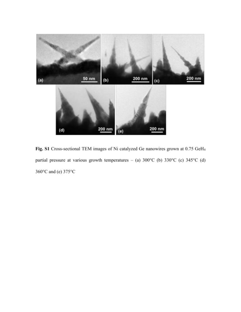
Fig. S1 Cross-sectional TEM images of Ni catalyzed Ge nanowires grown at 0.75 GeH4 partial pressure at various growth temperatures – (a) 300C (b) 330C (c) 345C (d) 360C and (e) 375C Fig. S2 Cross-sectional TEM images of Ni catalyzed Ge nanowires grown at 330 C and various GeH4 partial pressures – (a) PGeH4 = 0.5 torr (b) PGeH4 = 0.6 torr (c) PGeH4 = 0.75 torr and (d) PGeH4 = 1.0 torr Supporting Information S3: In order to further confirm the hypothesis that both VSS and VLS nanowire growth kinetics in the higher temperature regime are limited by vapor phase transport (e.g. of GeH4 precursor to the nanowires) for the typical operating conditions of our CVD reactor a rough estimate was made of the amount of Ge deposited per unit substrate area in the form of nanowires. This estimate was performed for both Au-catalyzed VLS growth and Ni-catalyzed VSS growth of Ge nanowires at the same growth temperature and GeH4 partial pressure. To compare the amount of Ge deposited, samples grown at 345C and 0.75 torr GeH4 partial pressure using Au and Ni nanoparticles were considered. To estimate the amount of Ge deposited on Au-catalyzed VLS-grown sample, the average nanowire densities (#/m2), diameters and lengths of the nanowires were calculated from SEM and TEM images of the samples. For Ni-catalyzed VSS growth, only the volume of Ge nanowires with straight morphology were included in the estimation. In equation 2, L denotes the average length of the nanowires; r and R denote the nanowire radii at the tip and the base of the nanowires. Taking into account the wire taper, the volume of Ge deposited per unit area (/m2) for both the samples was estimated as – V ( /# m)x V 2 G e N (1) W V 13RRrr 2 N 2 (2) W For Au catalyzed VLS-grown sample, the volume was calculated as 7x10⁷ nm3/m2 in the form of Ge nanowires. For Ni catalyzed VSS grown sample, the corresponding Ge volume was estimated as 2x10⁶ nm3/m2. A significant amount of Ge is also deposited in the form of kinked nanowires on the VSS-grown sample, which was not included in the calculation here. These estimates indicate that a comparable amount of Ge is deposited for both VSS and VLS, in spite of the much smaller axial length of VSS-grown (546 nm for the straight wires) versus VLS-grown (6250 nm) Ge nanowires at 345°C. This further supports the conclusion that, in the higher temperature VSS growth regime, the vapor phase transport is rate limiting, rather than factors associated with the catalyst.
