File
advertisement
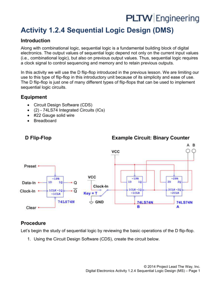
Activity 1.2.4 Sequential Logic Design (DMS) Introduction Along with combinational logic, sequential logic is a fundamental building block of digital electronics. The output values of sequential logic depend not only on the current input values (i.e., combinational logic), but also on previous output values. Thus, sequential logic requires a clock signal to control sequencing and memory and to retain previous outputs. In this activity we will use the D flip-flop introduced in the previous lesson. We are limiting our use to this type of flip-flop in this introductory unit because of its simplicity and ease of use. The D flip-flop is just one of many different types of flip-flops that can be used to implement sequential logic circuits. Equipment Circuit Design Software (CDS) (2) - 74LS74 Integrated Circuits (ICs) #22 Gauge solid wire Breadboard D Flip-Flop Example Circuit: Binary Counter Procedure Let’s begin the study of sequential logic by reviewing the basic operations of the D flip-flop. 1. Using the Circuit Design Software (CDS), create the circuit below. © 2014 Project Lead The Way, Inc. Digital Electronics Activity 1.2.4 Sequential Logic Design (MS) – Page 1 a) Start the simulation. VCC 5V Que S1 Not_Que 2.5 V Key = P GND 4 2.5 V U1A ~1PR 2 1Q 5 ~1Q 6 1D VCC 3 5V 1CLK S2 ~1CLR 1 GND 74LS74D Key = T VCC 5V S3 Key = C GND b) Set the input switches P and C to 5v. Again, since PR and CLR are active low inputs, this will make them both inactive. Toggle the input T several times. The circuit should behave exactly like the circuit in Activity 1.1.6, c) Set the input switch P to GROUND and C to 5v. What is the state of the two outputs? Que On /Not_Que Off d) Toggle the input T several times. Record what effect this has on the two outputs. It has NO effect. © 2014 Project Lead The Way, Inc. Digital Electronics Activity 1.2.4 Sequential Logic Design (MS) – Page 2 e) Set the input switch P to 5v and C to GROUND. What is the state of the two outputs? Que Off Not_Que ON f) Toggle the input T several times. Record what effect this has on the two outputs. It has NO effect. 2. Let us examine a simple binary counter. Counters are one of the most common applications of flip-flops. The circuit that we will be observing is called a two-bit binary counter. The counter will count from zero (00 in binary) to three (11 in binary). 3. Using the Circuit Design Software (CDS), enter the two-bit binary counter shown below. Use a switch for the input Clock-In and probes for the outputs A and B. a) Start the simulation. VCC A 5V B 2.5 V 4 VCC 10 U1A ~1PR 5V 2 S1 3 1CLK 1Q 12 ~1Q 6 11 ~1CLR 1 U1B ~2PR 5 1D 2.5 V 2Q 9 ~2Q 8 2D 2CLK ~2CLR 74LS74N 13 74LS74N Key = Space GND © 2014 Project Lead The Way, Inc. Digital Electronics Activity 1.2.4 Sequential Logic Design (MS) – Page 3 b) In Activity 1.1.6 we learned that the output on the first flip-flop (A) changes only when the Clock-In goes from low to high. Toggle the input Clock-In (switch T) until both outputs A and B are both low and switch T is low. Now cycle switch T (Cycle means to toggle from low to high back to low) and record what effect this has on the two outputs in the table below. Clock-In Initial Values st 1 Cycle of switch T 2nd Cycle of switch T 3rd Cycle of switch T 4th Cycle of switch T 5th Cycle of switch T 6th Cycle of switch T 7th Cycle of switch T 8th Cycle of switch T 9th Cycle of switch T A 0 B 0 0 1 1 0 0 1 1 0 0 1 0 1 0 1 0 1 0 1 Based on these results, explain the pattern that you observe in the two outputs. Output A either has two instances of On next to each other or two Off next to each other. Output B is alternating between 0 and 1. 4. Using the Circuit Design Software (CDS), modify the circuit used in step (1) so that it matches that shown below. a. The first modification is to replace the switch input with a CLOCK_VOLTAGE. This change will result in the input being continuously toggled. Be sure the CLOCK_VOLTAGE is set to 5 volts, 50% duty cycle, 60 Hz. b. The second modification is to add a four-channel oscilloscope set up to view the three signals A, B, and Clock-In. c. Be sure to set the oscilloscope’s time-base to 20ms/div and the vertical bases of the four channels to 10volts/div. Also, adjust the Y position of the three channels such that the four signals are all clearly visible. © 2014 Project Lead The Way, Inc. Digital Electronics Activity 1.2.4 Sequential Logic Design (MS) – Page 4 A B CLK d. Start the simulation and let it run until you have captured several periods of each signal. e. Using the oscilloscope’s markers, measure the period of the three signals. Use this data to calculate the frequency for each signal. Record your data in the table below. Be sure to use the correct units. Signal Period Frequency Clock-In 16.5ms 60Hz B 33.5ms 30Hz A 66.4ms 15Hz © 2014 Project Lead The Way, Inc. Digital Electronics Activity 1.2.4 Sequential Logic Design (MS) – Page 5 f. Based on these results, explain the relationship of the period and frequency between the three signals. Was this expected? The Period of each is half of the one before so A is two times B and B two times Clock-In. The Frequency is the opposite, A is half B and B half Clock-in, so the Period is inversely proportional to the Frequency. 5. Analyze the 4-bit binary counter shown below to determine the frequency and period for the signals A, B, C, and D. Use the table shown below to record your answers. Signal Clock-In D C B A Period 1ms 2.4ms 4.1ms 7.9ms 15.9ms Frequency 1000 Hz 417Hz 243Hz 126Hz 62Hz 6. With such a fast clock speed (1kHz) it is very difficult to see the binary count. Change the clock frequency to something that allows you to see the 4 probes transition more slowly in the simulation. Can you count to 15 in binary? What was the clock frequency that was best for you? 100Hz 7. Using the pin diagram on the datasheet for the 74LS74 D flip-flop, create the 4-Bit counter you explored in this activity on your protoboard. Wire the four outputs to (Y3, Y2, Y1, Y0) of your protoboard. Wire the DIO3 to the CLK input of the first flip-flop. © 2014 Project Lead The Way, Inc. Digital Electronics Activity 1.2.4 Sequential Logic Design (MS) – Page 6 Using the myDAQ to generate a clock signal. 8. With the protoboard plugged into the myDAQ, the myDAQ provides a number of instruments that assist with design and measurement. We will use the NI ELVISmx Digital Writer “DigOut” to generate a clock signal 9. Open National Instruments > NI ELVISmx Instrument Launcher. Select “DigOut”. 10. Settings: a. Lines to Write (0-3) b. Pattern (Ramp 0-15) c. Run Continuously 11. When you select “Run” the Digital Writer will send a signal that can be used as a clock signal to DIO3. 12. To utilize a faster frequency, switch to DIO2 DIO1 or DIO0. 13. Have your instructor verify the counter is functioning. Conclusion © 2014 Project Lead The Way, Inc. Digital Electronics Activity 1.2.4 Sequential Logic Design (MS) – Page 7 1. The 2-Bit and 4-Bit counters you explored in this activity are referred to as “divide by two” counters. Explain the relationship between each consecutive flip flop and the order in which they are laid out in the design from right to left that creates a binary count. Each flip-flop is half the speed from the previous one 2. If you added a 5th bit, what would you guess is the highest number you could count to? 75 3. Can you think of 3-5 everyday items/products that might have a counter incorporated in them? Pedometer, altimeter, odometer, barometer © 2014 Project Lead The Way, Inc. Digital Electronics Activity 1.2.4 Sequential Logic Design (MS) – Page 8

