twepp09_paper_ssilva_20090918 - Indico
advertisement
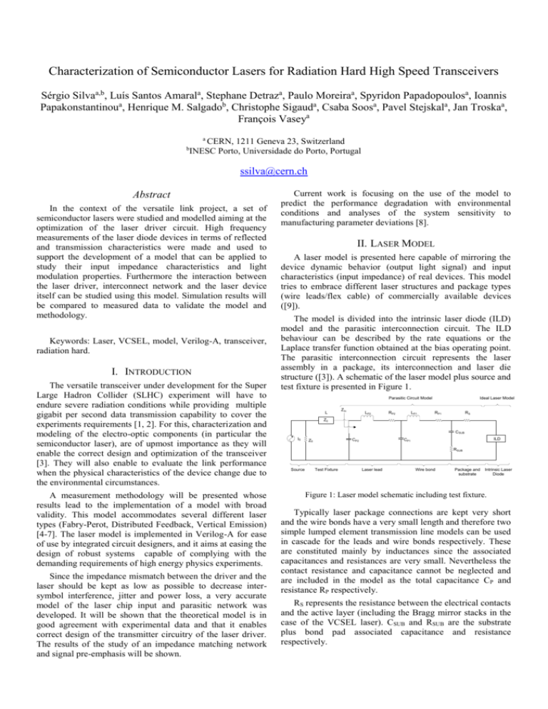
Characterization of Semiconductor Lasers for Radiation Hard High Speed Transceivers Sérgio Silvaa,b, Luís Santos Amarala, Stephane Detraza, Paulo Moreiraa, Spyridon Papadopoulosa, Ioannis Papakonstantinoua, Henrique M. Salgadob, Christophe Sigauda, Csaba Soosa, Pavel Stejskala, Jan Troskaa, François Vaseya a b CERN, 1211 Geneva 23, Switzerland INESC Porto, Universidade do Porto, Portugal ssilva@cern.ch Abstract In the context of the versatile link project, a set of semiconductor lasers were studied and modelled aiming at the optimization of the laser driver circuit. High frequency measurements of the laser diode devices in terms of reflected and transmission characteristics were made and used to support the development of a model that can be applied to study their input impedance characteristics and light modulation properties. Furthermore the interaction between the laser driver, interconnect network and the laser device itself can be studied using this model. Simulation results will be compared to measured data to validate the model and methodology. Keywords: Laser, VCSEL, model, Verilog-A, transceiver, radiation hard. I. INTRODUCTION The versatile transceiver under development for the Super Large Hadron Collider (SLHC) experiment will have to endure severe radiation conditions while providing multiple gigabit per second data transmission capability to cover the experiments requirements [1, 2]. For this, characterization and modeling of the electro-optic components (in particular the semiconductor laser), are of upmost importance as they will enable the correct design and optimization of the transceiver [3]. They will also enable to evaluate the link performance when the physical characteristics of the device change due to the environmental circumstances. A measurement methodology will be presented whose results lead to the implementation of a model with broad validity. This model accommodates several different laser types (Fabry-Perot, Distributed Feedback, Vertical Emission) [4-7]. The laser model is implemented in Verilog-A for ease of use by integrated circuit designers, and it aims at easing the design of robust systems capable of complying with the demanding requirements of high energy physics experiments. Since the impedance mismatch between the driver and the laser should be kept as low as possible to decrease intersymbol interference, jitter and power loss, a very accurate model of the laser chip input and parasitic network was developed. It will be shown that the theoretical model is in good agreement with experimental data and that it enables correct design of the transmitter circuitry of the laser driver. The results of the study of an impedance matching network and signal pre-emphasis will be shown. Current work is focusing on the use of the model to predict the performance degradation with environmental conditions and analyses of the system sensitivity to manufacturing parameter deviations [8]. II. LASER MODEL A laser model is presented here capable of mirroring the device dynamic behavior (output light signal) and input characteristics (input impedance) of real devices. This model tries to embrace different laser structures and package types (wire leads/flex cable) of commercially available devices ([9]). The model is divided into the intrinsic laser diode (ILD) model and the parasitic interconnection circuit. The ILD behaviour can be described by the rate equations or the Laplace transfer function obtained at the bias operating point. The parasitic interconnection circuit represents the laser assembly in a package, its interconnection and laser die structure ([3]). A schematic of the laser model plus source and test fixture is presented in Figure 1. Parasitic Circuit Model L ZIn LP2 LP1 RP2 Ideal Laser Model RP1 RS Z0 CSUB IS CP2 Z0 ILD CP1 RSUB Source Test Fixture Laser lead Wire bond Package and substrate Intrinsic Laser Diode Figure 1: Laser model schematic including test fixture. Typically laser package connections are kept very short and the wire bonds have a very small length and therefore two simple lumped element transmission line models can be used in cascade for the leads and wire bonds respectively. These are constituted mainly by inductances since the associated capacitances and resistances are very small. Nevertheless the contact resistance and capacitance cannot be neglected and are included in the model as the total capacitance CP and resistance RP respectively. RS represents the resistance between the electrical contacts and the active layer (including the Bragg mirror stacks in the case of the VCSEL laser). CSUB and RSUB are the substrate plus bond pad associated capacitance and resistance respectively. Under operating conditions (bias current much higher than the threshold current), the laser diode depletion region is very conductive and so the ILD impedance is very small and is, for input impedance calculation purposes, much lower than RS and thus negligible ([5]). Therefore the laser input impedance can be obtained right of the arrow pointer with the ILD short-circuited, as illustrated in Figure 1. For the intrinsic laser diode it is assumed that since we are only interested in the mean photon densities it is possible to model the laser using only a single rate equation. Typical telecom lasers operate in a single-longitudinal mode which makes them suitable for high-bit-rate fiber optic communications ([3, 5]). This also makes the approximation of the laser behavior by a single pair of rate equations very accurate. This is the case for the DFB and VCSEL lasers but not FP. In the case of the FP laser, the photon density accounted for in the rate equation is the mean densities between all modes. Nevertheless, if one is interested solely in the dynamics of the output light power, this approximation is still valid. For small modulation currents (iModulation < IBias ), the intrinsic laser diode can be modelled using its transfer function. Obtaining the steady-state equation for a specific bias current, it is then possible to linearize of the rate equations around the operating point ([5]). From this, the laser transfer function is easily calculated as the Laplace transform of these linearized rate equations ([5]). For large signals (iModulation ≈ IBias ), the full differential rate equations must be used which can make the simulation process slower. III. PARAMETER EXTRACTION The laser model parameters can be extracted using SParameter measurements (reflection and transmission characteristics) conducted using a network vector analyzer ([9]) or the relative intrinsic noise spectrum curves measured with a spectrum analyser. Starting from known parameters obtained for similar lasers in the literature, the optimization algorithm (constrained parameter curve fit) tries to find the set of parameters that lies within pre-determined bounds and searches for the minimum square error of a set of curves. Since the input impedance measurement is decoupled from the ILD (the ILD is considered as having very low impedance), the S11 (reflection) measurements are used to obtain the parasitic circuit parameters. The ILD rate equation parameters, on the other hand, can be extracted using two methods: frequency subtraction ([4, 9]) and relative intensity noise spectrum fit ([10]). The frequency subtraction method was presented in [9] and proceeds using the S21 (transmission) measured at different bias currents and then fitting a laser frequency response model obtained using the laser rate equations noting that ([4, 2]): 𝐻𝐺𝑙𝑜𝑏𝑎𝑙 (𝑓, 𝐼𝐵𝑖𝑎𝑠 ) 𝐻𝐺𝑙𝑜𝑏𝑎𝑙 (𝑓, 𝐼𝑅𝑒𝑓 ) = 𝐻𝑃𝐶 (𝑓)𝐻𝑇𝐹 (𝑓)𝐻𝐼𝐿𝐷 (𝑓, 𝐼𝐵𝑖𝑎𝑠 ) = 𝐻𝑃𝐶 (𝑓)𝐻𝑇𝐹 (𝑓)𝐻𝐼𝐿𝐷 (𝑓, 𝐼𝑅𝑒𝑓 ) 𝐻𝐼𝐿𝐷 (𝑓, 𝐼𝐵𝑖𝑎𝑠 ) (1) 𝐻𝐼𝐿𝐷 (𝑓, 𝐼𝑅𝑒𝑓 ) The laser transfer function is given as a function of the SParameters by: 𝐻𝐺𝑙𝑜𝑏𝑎𝑙 (𝑓, 𝐼𝐵𝑖𝑎𝑠 ) = 𝑆21 (𝑓, 𝐼𝐵𝑖𝑎𝑠 )(1 − 𝑆11 (𝑓)), (2) So the quotient (subtraction with log operator) between the laser response (HGlobal (f, IBias )) at different currents above threshold (IBias , IRef ) is not affected by the parasitic circuit transfer function (HPC (f)) or the laser assembly transfer function (HTF (f)) since these are not dependent on bias current, and is simply the quotient of the ILD transfer functions which is known and a function of the model parameters. The HILD (f, IBias ) function can be approximated by the following equation ([4, 5]): 𝐻𝐼𝐿𝐷 (𝑓, 𝐼𝐵𝑖𝑎𝑠 ) 𝑓𝑟2 ≈ 2 𝐻𝐼𝐿𝐷 (0, 𝐼𝐵𝑖𝑎𝑠 ) 𝑓𝑟 − 𝑓 2 + 𝑗𝑓𝑓𝑑 (3) In this equation, fr (resonant frequency) and fd (damping frequency) are a function of the ILD model parameters and bias current, as dictated by the rate equations. This enables the estimation of the following ILD rate equation parameters: V, volume; g0, gain slope constant; ε, gain compression factor; N0m, carrier density at transparency; β, spontaneous emission factor; Γ, optical confinement Factor; τp, photon life time; τn, electron life time. The ILD parameter extraction is made by adjusting a set of curves obtained for the ratio of transfer functions for two different currents to the ones obtained with measured data. Using a set of curves obtained for different pairs of operating currents enhances the fitting robustness. A final tuning using the global model response and can be carried out as the last step (Figure 2). RIN(f, IBias) S21(f, IBias) S-Parameters Intrinsic Laser Diode Parameters Extraction ILD Parameters Global Response Parameters Adjustment Test Fixture Deembedding S(f, IBias) S11(f, IBias) Parasitic Circuit Parameters Extraction Complete Model Parameters PC Parameters Open, Short & Load Test Fixture S-Parameters Figure 2: Parameter extraction algorithm. The relative intensity noise spectrum method uses the measured noise spectrum curves (RIN(f)) of the laser using a spectrum analyzer and a model obtained using the rate equations for this curves. The laser parameter estimation is then a curve fitting procedure using the equation bellow: 𝑅𝐼𝑁(𝑓) 𝑓𝑟4 𝑓 2 + 𝑓𝑑2 ≈ 2 2 𝑅𝐼𝑁(0) 𝑓𝑑 (𝑓 + 𝑓𝑟2 )2 + 𝑓 2 𝑓𝑑2 (4) Again, fr and fd are a function of the ILD model parameters and bias current. As an initial guess, the parameters obtained using methods such as frequency subtraction should be used. Otherwise the published laser manufacturer parameters can be used if available. Both parameter extraction methods provide a way to obtain the ILD rate equation parameters. With these parameters and the rate equations, the entire steady state and dynamic behaviour of the laser can be described mathematically and thus be incorporated in a simulation software. IV. RESULTS Several types of different laser devices were measured and its model parameters estimated by the method here described. Figure 3 presents a summary of the extracted parameters. Here device 1 is a Fabry-Perot long wavelength laser, device 2 is a VCSEL long wavelength laser and the remaining devices are short wavelength VCSEL lasers. Devices 5 and 6 are the same laser device but with wire leads and flex cable connections respectively. The values for the parameters that are associated to the bond wire (CP1, LP1 and RP1) are similar for all devices. This is to be expected since they all use the same package type and are at this level very similar. The exception being the FP laser whose parameters are higher than the mean values. It is interesting to see that the active area resistance is clearly higher in the VCSEL and even higher in the short wavelength laser, as it does not use a buried tunnel heterojunction structure. The inductance values agree with the ones expected for short connections but the capacitance and resistance values are higher than the expected ones. This might be due to capacitive effects between the wires and package that were not considered explicitly in the parasitic model. And as for the resistance RP2, contact and solder imperfections might be responsible for this high value. For the ILD parameter values, the lasers of the same family show agreement between them (3, 4 and 5, 6) as it was to be expected. More so between the devices 5 and 6 since they are basically the same laser device with different electrical packages. The FP laser has the highest active volume value which is in agreement with its internal structure. The VCSEL long wavelength laser (device 2) has an active volume that is larger than the short wavelength lasers, a consequence of the internal structure for this type of lasers. For simulation purposes the laser parasitic circuit and ILD model are implemented using Verilog-A, which is a suitable format for numerous simulations packages ([9]). With this model and the extracted parameters it is possible to compare the measured transfer function with the results obtained with the model (shown here for the case of a long wavelength VCSEL laser). As it can be seen, the model agrees with the measured data to a good degree for the transfer function (Figure 4) at several bias currents (I1< I2< I3< I4) and for the eye diagram (Figure 5; blue measured, red simulation). With this model it is possible to study and optimize the electrical network that connects a laser driver to the laser and the way the bias current is supplied to it. Furthermore, the high magnetic field devices are subjected to in the particle detector makes impossible to use ferromagnetic components, making it necessary to use alternative configurations for the supply of the laser bias currents. This includes the use of ceramic/air core inductors or microstrip inductors. Both solutions represent a loss of performance regarding a solution with ferromagnetic core inductors and need to be studied. Laser drivers are typically sensitive to signal reflections caused by the impedance mismatch between the driver output -18 0.8 1 2 3 4 5 4 0.2 2 0 0 1 2 3 4 5 g0 4 -1 3 0.4 6 V 6 m pF 50 0 Cs 0.6 x 10 5 6 3 Rs -12 x 10 8 m s 100 3 2 1 2 3 4 5 1 6 1 -23 8 3 4 4 2 2 0 0 0 2 3 4 5 6 1 2 3 4 5 6 3 4 5 6 N0m 3 4 2 1 6 m nH pF Lp1 6 2 24 x 10 4 -3 Cp1 6 8 m 8 x 10 2 1 1 2 3 4 5 0 6 1 2 3 4 5 6 -3 2 3 Rp1 Cp2 - pF 1 2 3 4 5 0 6 5 3 4 5 6 3 4 Device 5 3 4 5 6 2 3 4 5 6 2 3 4 5 6 n 4 1 1 1 6 ps 0 0 6 p 1.5 2 2 2 2 2 4 1 1 0.04 0.02 Rp2 nH 2 6 3 1 1 Lp2 4 1 0.5 0 0.06 ns 1 0 1.5 2 0.5 0.08 - 1 x 10 0.5 1 2 2 3 Device Figure 3: Parasitic & ILD model parameters. 4 5 6 0 1 2 3 4 5 6 for a laser, is to charge and discharge the parasitic capacitances faster. and laser input load. Matching circuit Measurement data & Complete Laser Model 5 0 ZM ZL -5 R2 Amplitude (dB) -10 -15 Data I1 -20 Data I2 -25 Data I3 -30 Data I4 Z0 IS R1 Laser R3 IA Model I1 -35 Model I2 -40 Model I3 Model I4 -45 0 1 2 3 4 5 6 Frequency (GHz) 7 8 9 R4 10 Figure 6: Impedance matching circuit. Figure 4: Transfer function of measured laser data and model simulations. 0.009 Eye Diagram 0.005 Current (A) Optical Output (mW) 1.0 0.5 0.0 0.002 -0.002 -0.005 -0.009 -0.5 0 100 200 300 400 Time (pS) -1.0 50 150 250 350 400 Time (pS) Figure 7, 8, 9, 10 shows the result of a simulation using a laser model and a Pi-resistive network to minimize the reflections back to the laser driver and a signal of 4.8GBPS. In Figure 8, the overshoot is the pre-emphasis effect and undershoot is caused by residual reflections. The high-frequency behaviour of a laser is significantly affected by the electrical parasitics of the laser die and package. The role of the pre-emphasis (or current peaking), 0.009 0.005 Current (A) It is possible to trade power transmission for reduced reflections by using a resistive matching network as the one in Figure 6. This network aims to obtain an impedance ZM ≈ Z0 by the use of a resistor net, trading signal reflection minimization for power transmission. The series damping resistor (R2 and R4) serves the dual purpose of damping reflections (that cause output distortion) and creating a stable load. Load stability is improved because the load presented by the laser can vary by a significant portion of its nominal value, whereas he combined load presented by the laser and the damping resistor varies by much less if the resistor take the bigger parcel of the series set. The circuit is able to effectively reduce the reflections into the source, but the resistors present in the circuit cause less power to be delivered to the laser. This is the trade off made: power transmission versus reflection reduction. So by reducing the mismatch between the laser input impedance and laser driver output impedance we are unavoidably reducing also the power that reaches the laser. A compromise is necessary to make maximize the power transfer while maintaining a suitable maximum level of interference due to signal reflections. 0.002 -0.002 -0.005 -0.009 0 100 200 300 400 Time (pS) Figure 8: Eye diagram for the current at network input (without matching circuit). 0.4 Optical Power (mW) Figure 5: Measured eye diagram and model simulations. Figure 7: Eye diagram for the current at network input (without matching circuit). 0.2 0.0 -0.2 -0.4 0 100 200 300 400 Time (pS) Figure 9: Eye diagram for the laser output (without pre- emphasis). Optical Power (mW) 0.4 0.2 0.0 -0.2 -0.4 0 100 200 300 400 Time (pS) Figure 10: Eye diagram for the laser output (with pre-emphasis). Current peaking allows modulation of lasers at higher rates without the need to reduce the laser parasitics. By using signal pre-emphasis (Figure 10) the rise and fall times are decreased from 80pS to 50pS. V. CONCLUSION Using simple assumptions, a broadly applicable model was developed that can be used with many different types of semiconductor lasers. This model is modular in order to separate the analysis made for package parasitic from the laser parameters. Very good agreement between the model and the measurements was obtained, which is fundamental for a correct study of the design of a robust transceiver with demanding requirements. The impact of the matching network is relevant for the behaviour of the laser driver as it might fail or reduce its performance if the level of the reflected signal is too high. For the laser output, these types of matching networks are not optimal and better improvements can be achieved when using signal pre-emphasis since resistive matching networks will always reduce the transmitted signal level. REFERENCES Hessey, N. (2008), “Overview and Electronics Needs of ATLAS and CMS High Luminosity Upgrades”, Proceeding of the TWEPP2008, Naxos, Greece. [2] Amaral, L. et al (2008), “Evalutation of Multi-Gbps Optical Transceivers for Use in Future HEP Experiments”, Proceeding of the TWEPP2008, Naxos, Greece. [3] Tucker, R.; Kaminow, I., "High-frequency characteristics of directly modulated InGaAsP ridge waveguide and buried heterostructure lasers", Journal of Lightwave Technology, vol.2, no.4, pp. 385-393, Aug 1984. [4] Morton, P. A.; et. al, “Frequency response subtraction for simple measurement of intrinsic laser dynamic properties,” IEEE Photon. Technol. Lett., vol. 4, pp. 133–136, Feb. 1992. [5] Salgado, H. M.; and O’Reilly, J. J.; “Volterra series analysis of distortion in semiconductor laser diodes,” Proc. Inst. Elect. Eng. J., vol. 138, no. 6, pp. 379–382, Dec. 1991. [6] Cartledge, J.C.; Srinivasan, R.C. (1997), "Extraction of DFB laser rate equation parameters for system simulation purposes", Journal of Lightwave Technology, vol.15, no.5, pp.852-860. [7] Bruensteiner, M.; Papen, G.C. (1999), "Extraction of VCSEL rate-equation parameters for low-bias system simulation," IEEE Journal of Selected Topics in Quantum Electronics, vol.5, no.3, pp.487-494. [8] Blokhin, S. A. et al (2006), “Experimental Study of Temperature Dependence of Threshold Characteristics in Semiconductor VCSELs Based on Submonolayer InGaAs QDs”, Journal of Semiconductors, Vol. 40, pp1232-1236. [9] Silva, Sergio; Salgado, Henrique M. (2009), "VCSEL laser characterization and modelling for future optical transceiver at the super large hadron collider", Proceedings of the 11th International Conference on Transparent Optical Networks (ICTON '09), pp.1-5, June 28-July 2, 2009. [10] Fukushima, T. et al (1991 b), "Relative intensity noise reduction in InGaAs/InP multiple quantum well lasers with low nonlinear damping", IEEE Photonics Technology Letters, vol. 3, no. 8, pp.688-693, August, 1991. [1]

