SI - AIP FTP Server
advertisement
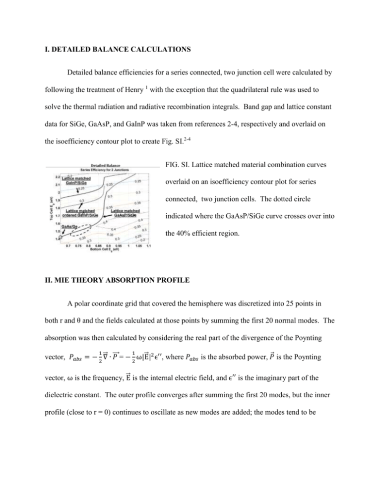
I. DETAILED BALANCE CALCULATIONS Detailed balance efficiencies for a series connected, two junction cell were calculated by following the treatment of Henry 1 with the exception that the quadrilateral rule was used to solve the thermal radiation and radiative recombination integrals. Band gap and lattice constant data for SiGe, GaAsP, and GaInP was taken from references 2-4, respectively and overlaid on the isoefficiency contour plot to create Fig. SI.2-4 FIG. SI. Lattice matched material combination curves overlaid on an isoefficiency contour plot for series connected, two junction cells. The dotted circle indicated where the GaAsP/SiGe curve crosses over into the 40% efficient region. II. MIE THEORY ABSORPTION PROFILE A polar coordinate grid that covered the hemisphere was discretized into 25 points in both r and θ and the fields calculated at those points by summing the first 20 normal modes. The absorption was then calculated by considering the real part of the divergence of the Poynting 1 1 ⃗ |2 ϵ′′, where 𝑃𝑎𝑏𝑠 is the absorbed power, 𝑃⃗ is the Poynting vector, 𝑃𝑎𝑏𝑠 = − 2 ⃗∇ ∙ ⃗⃗⃗ 𝑃 = − 2 ω|E ⃗ is the internal electric field, and ϵ′′ is the imaginary part of the vector, ω is the frequency, E dielectric constant. The outer profile converges after summing the first 20 modes, but the inner profile (close to r = 0) continues to oscillate as new modes are added; the modes tend to be highly structured around the origin. Thus, the seven lowest r values around the origin were discarded. For a 2 µm radius sphere, the Mie theory results are plotted in Fig. S2 alongside a simple Beer-Lambert (B-L) profile. For the Mie model, the plane wave is incident from the x direction (θ = 90o on the plot), and the X-Z optical generation cross section is shown. The Y-Z cross section is similar. For the B-L absorption profile, the generation is assumed to decay exponentially into the material with a decay length of 𝛼(𝜔) = 2𝜔𝜅, where ω is the frequency and κ is the imaginary part of the index of refraction. FIG. S2. Polar coordinate plots comparing Mie Theory and Beer-Lambert absorption for the upper GaAs0.9P0.1 cell. III. SOLVING FOR THE DEPLETION REGION LIMITS In the analytical model described in the text, the limits of the depletion region may be found by maintaining charge conservation: 𝑁𝐴 (𝑑23 − 𝑥43 ) = 𝑁𝐷 ((𝑑2 + 𝑥2 )3 − 𝑑23 ) (S1) and by then solving Poisson’s equation in spherical coordinates (assuming angle invariance): 𝑑𝑉 2 1 𝑑(𝑟 𝑑𝑟 ) 𝑟2 𝑑𝑟 = 𝜌 𝜀 (S2) IV. THE DIFFUSION EQUATION IN RADIAL COORDINATES The diffusion equation may be written in spherical coordinates as follows (assuming angle invariance): 2 n, p n, p 1 L2n , p r 2 d (r 2 dn, p ) dr n, p 0 e ( r ( d1 d 2 )) dr L2n , p Dn , p (S3) where n,p is the minority carrier in the given region, L is the diffusion length of the carriers, and D is the diffusion coefficient. V. SURFACE RECOMBINATION VELOCITY EFFECTS Fig. S3 compares the light IV performance of a device as the SRV is varied. The structure shown is a 3 µm hemisphere, but, as might be expected, larger structures were even less affected by the SRV. Fig. S3. Light IV curve of the shell as the outer (r = d1+d2) and inner (r = 0) surface recombination velocities are varied. The velocities are both set to have the values indicated. VI. SERIES RESISTANCE EFFECTS Tandem cells incorporate a tunnel junction to facilitate current transport between the two subcells. While this junction is highly doped to allow for low resistance tunneling, it will still have a finite resistance. Thus, a series resistance was added to the tandem model to explore the effects of a nonideal tunnel junction. For resistances of 0.7 and 1 Ω cm2, the tandem efficiencies of the cells in Table 1 remained above 32 and 33%, respectively. However, for larger values of series resistance, the cell efficiency rapidly began to fall, as seen in Fig. S4. FIG. S4. The effect of series resistance (Rs) on the performance of the second tandem cell in Table 1. VII. 2D VS. 3D OPTICAL SIMULATIONS Optical absorption simulations were performed at 50 nm steps for both a two dimensional model and a full three dimensional model with periodic side boundary conditions, a perfectly absorbing top boundary, and a perfectly reflecting base. The absorption profiles were calculated as described in the text and the cross sections were compared, as seen in Fig S5. The absorption features that were visible in the 3D structure were mirrored in the two dimensional model, as demonstrated at one wavelength (850 nm) in b. Overall, The GaAs1-xPx absorption for the 2D and 3D models were nearly identical while the SixGe1-x absorption was appreciably lower in the 850-1100 nm range for the 3D model due to the smaller physical cross section. As experiments have shown that wires can absorb the majority of light within this range with the incorporation of scattering particles and anti-reflective coatings5, the higher absorption of the 2D model was assumed to be possible. FIG. S5. 2D vs. 3D optical simulation comparison (a) Comparison of 2D (TE and TM) and 3D absorption rates in the core and shell of the structure shown in Fig. 11 as a function of wavelength.(b) Absorption profiles at 850 nm for the 2D and 3D cases. VIII. FINE VS. COURSE OPTICAL SIMULATIONS Due to the length of time required to run the optical simulations and, more significantly, to interpolate the finite-difference-time-domain grid onto the finite element grid, optical simulations were run in 50 nm steps for the optoelectronic simulations. However, to make sure that no significant features were missing in the optical response, optical simulations were also run in 25 nm steps as a check. A comparison of the two absorption profiles for the different wavelength spacings is shown in Fig. S6, and the differences in “ideal” (IQE=1) short circuit densities that would be expected for the two profiles are listed in Table SI. The largest difference between the two values is 1% for the window layers, which do not contribute to the overall current of the device. The difference in shell and wire absorption between the two profiles is less than 1%. FIG. S6. Comparison of the absorption profiles for FDTD optical simulations run at 25 nm wavelength steps vs. 50 nm wavelength steps. TABLE SI. Calculated ideal (IQE=1) JSC of layers under course (50 nm wavelength step) and fine (25 nm step) simulations. Structure Region Conformal Window Shell Wire Window Shell Wire Window Shell Wire Hemisphere Sphere Course JSC (mA/cm2) 2.67 20.49 23.32 2.02 21.53 21.07 2.04 21.27 22.92 Fine JSC (mA/cm2) % Difference 2.67 20.59 23.46 2.00 21.52 20.92 2.02 21.30 22.94 0 0.5 0.6 1 0.04 0.7 1 0.1 0.09 IX. OPTICAL LOSS AND ABSORPTION MECHANSIMS The optical absorption and loss mechanisms were explored through the course of optical simulations and are outlined in Figure S7. While the ray tracing limit will not be valid for the longer wavelengths simulated, the figure is meant as more of general guide. FIG. S7. Cartoon depicting the loss and absorption mechanisms in a wire array tandem cell. 1: Reflection off of the III-V/infill interface. 2: Light that misses the cell entirely. 3: Reflection off of the wire surface. 4: Light absorbed directly in the III-V. 5: Light scattered into the wire. 6: Light guided through the III-V into the wire and absorbed. X. PITCH DEPENDENCE Optical simulations were performed at a variety of wire pitches in order to maximize the current matched photocurrent. Results are plotted in Fig. S8. FIG. S8. Plot of the relative absorption in the core and shell for all three structures for varying pitch. XI. INTERPOLATING FDTD GRID ONTO FEM GRID In order to facilitate geometrical correspondence from the two-dimensional optical simulations to the three-dimensional device physics model, after summing and weighting the single wavelength simulations, the overall generation profile was weighted by 𝑅2 𝑟 where R is equal to half of the pitch and r is the profile's x coordinate. Thus when integrated cylindrically, the profile yields the same idealized JSC as when integrated in two dimensions. The modified profile was then interpolated onto a finite element grid for device physics simulations. XII. DEVICE PHYSICS MODEL PARAMETERS Physical Constant Tunnel junction model: Ratio of effective Richardson constant to free electron Richardson constant Tunnel junction model: Tunneling mass Additional notes: Value 0.21 (electrons), 0.4 (holes) 0.05 (electrons), 0.14 (holes) SixGe1-x, GaAs1-xPx, and GaxIn1-xP data was generated through Sentaurus. Full Fermi statistics were assumed. Thermionic emission was calculated at all heterojunctions using the model of Schroeder 6 and assumed A = 2, B = 4, and C =1 for both electrons and holes. Both intra- and interband tunneling were calculated at the tunnel junction . XIII. SURFACE RECOMBINATION VELOCITY As a final test of the three geometries, the surface recombination velocity of the Ga0.56In0.44P surface, the Si0.1Ge0.9/ Ga0.56In0.44P interface, and all III-V dielectric interfaces was uniformly varied. The results on device performance are shown in Table SII. The conformal structure’s behavior is relatively unaffected by the SRV change as the GaAs0.9P0.1 is completely coated with the Ga0.56In0.44P window. In fact, the efficiency goes up slightly at high SRVs due to an increase in fill factor. The contact is set as a small area at the bottom of the wire, but, when the SRV is high, the contact effectively extends to the entire outer surface. Minority carriers are reflected by the window layer, but majority carriers recombine at the surface. The hemisphere and sphere designs, on the other hand, experience a drop in performance with increasing SRV due to increasing recombination at the III-V dielectric interface. TABLE SII. Device performance as a function of surface recombination velocity SRV (cm/s) VOC (V) Eff (%) Conformal 104 1.23 21.3 106 1.20 21.4 Hemisphere 104 1.27 20.9 6 10 1.11 17.0 4 Sphere 10 1.24 21.7 106 1.06 17.6 XIV. DIFFUSION VS. RECOMBINATION Fig S9 plots the SRH recombination for one of the scenarios considered. At higher lifetimes, the carriers diffuse throughout the shell, leading to more homogeneous recombination whereas the carriers are more localized for the short diffusion length devices. . FIG. S9. Shockley-Reed-Hall recombination for τn = 500 or 5 ps in the GaAs0.9P0.1 cell for an array with a 7 µm pitch REFERENCES 1 2 3 4 5 6 C. H. Henry, Journal of Applied Physics 51, 4494 (1980). R. Braunstein, A. R. Moore, and F. Herman, Physical Review 109, 695 (1958). I. Vurgaftman, J. R. Meyer, and L. R. Ram-Mohan, Journal of Applied Physics 89, 5815 (2001). R. R. King, C. M. Fetzer, K. M. Edmondson, D. C. Law, P. C. Colter, H. L. Cotal, R. A. Sherif, H. Yoon, T. Isshiki, D. D. Krut, G. S. Kinsey, J. H. Ermer, S. Kurtz, T. Moriarty, J. Kiehl, K. Emery, W. K. Metzger, R. K. Ahrenkiel, and N. H. Karam, in METAMORPHIC III-V MATERIALS, SUBLATTICE DISORDER, AND MULTIJUNCTION SOLAR CELL APPROACHES WITH OVER 37% EFFICIENCY, Paris, France, 2004. M. D. Kelzenberg, S. W. Boettcher, J. A. Petykiewicz, D. B. Turner-Evans, M. C. Putnam, E. L. Warren, J. M. Spurgeon, R. M. Briggs, N. S. Lewis, and H. A. Atwater, Nature Materials 9, 239 (2010). D. Schroeder, Modelling of Interface Carrier Transport for Device Simulation (Springer-Verlag Kg, 1994).

