opAmpDesign
advertisement

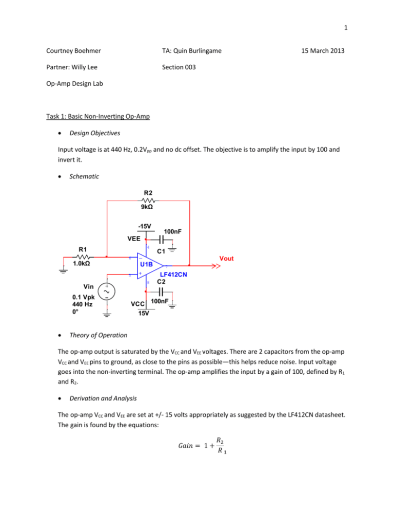
1 Courtney Boehmer TA: Quin Burlingame Partner: Willy Lee Section 003 15 March 2013 Op-Amp Design Lab Task 1: Basic Non-Inverting Op-Amp Design Objectives Input voltage is at 440 Hz, 0.2Vpp and no dc offset. The objective is to amplify the input by 100 and invert it. Schematic R2 9kΩ -15V 100nF VEE 4 R1 1.0kΩ U1B 5 8 Vin 0.1 Vpk 440 Hz 0° C1 6 Vout 7 LF412CN C2 VCC 100nF 15V Theory of Operation The op-amp output is saturated by the VCC and VEE voltages. There are 2 capacitors from the op-amp VCC and VEE pins to ground, as close to the pins as possible—this helps reduce noise. Input voltage goes into the non-inverting terminal. The op-amp amplifies the input by a gain of 100, defined by R1 and R2. Derivation and Analysis The op-amp VCC and VEE are set at +/- 15 volts appropriately as suggested by the LF412CN datasheet. The gain is found by the equations: 𝐺𝑎𝑖𝑛 = 1 + 𝑅2 𝑅1 2 Gain is equal to 100. If R1 is 1KΩ, then R2 is 99KΩ. Experimental Results Ch 1 is the voltage input. Ch 2 is the voltage output. Our gain is found by 𝑔𝑎𝑖𝑛 = 𝑔𝑎𝑖𝑛 = 𝑉𝑂𝑈𝑇 𝑉𝐼𝑁 19.7 𝑣𝑜𝑙𝑡𝑠 = 92.056 . 214 𝑣𝑜𝑙𝑡𝑠 The ideal gain was -100. The percent error is 𝑝𝑒𝑟𝑐𝑒𝑛𝑡 𝑒𝑟𝑟𝑜𝑟 = |𝐴𝑝𝑝𝑟𝑜𝑥𝑖𝑚𝑎𝑡𝑒 𝑉𝑎𝑙𝑢𝑒 − 𝐸𝑥𝑎𝑐𝑡 𝑉𝑎𝑙𝑢𝑒| ∗ 100 |𝐸𝑥𝑎𝑐𝑡 𝑉𝑎𝑙𝑢𝑒| 3 𝑝𝑒𝑟𝑐𝑒𝑛𝑡 𝑒𝑟𝑟𝑜𝑟 = |92.056 − 100| ∗ 100 = 7.44% |100| Discussion of Results and Concluding Thoughts According to our task1 experiment, we measure input Vpk-pk and output Vpk-pk and calculate the gain of our op amp circuit design. We utilize the percent error analysis to observe the percent difference of theoretical result and experimental result. Our circuit worked pretty well since we had 92.056 gain in attempt to get 100, resulting in 7.44%. There could be various sources of error that have caused this, including several major human errors such as choosing resistor with relatively bad tolerance. The nominal value of resistor we used is different from the actual value of resistors we used. Nonetheless, we had pretty good result. Task 2: Difference Amplifier Design Objectives There are two input voltages. VL is 0.1 VPP at 440 Hz and 0.1Vpp at 1560 Hz, with no dc offset. VR is 0.1 VPP at 440 Hz and 0.1Vpp at 3520 Hz, also with no dc offset. The objective is to amplify VL by 100 and add it to VR amplified by -100. Schematic R2 100kΩ -15V VEE C1 100nF 4 R1 VR2 0.05 Vpk 440 Hz 0° VR1 0.05 Vpk 1560 Hz 0° 1.0kΩ U1B 6 7 R3 5 1.0kΩ VL2 0.05 Vpk 440 Hz 0° VL1 0.05 Vpk 3520 Hz 0° 8 R4 99kΩ LF412CN C2 100nF VCC 15V Vout 4 Theory of Operation The op-amp output is saturated by the VCC and VEE voltages. There are 2 capacitors from the op-amp VCC and VEE pins to ground, as close to the pins as possible—this helps reduce noise. VL goes to the non-inverting op-amp pin. VL is amplified based on the ratio of R3 and R4. VR goes to the inverting opamp pin. VR is amplified and inverted based on the ratio of R1 and R2. The output is VL with a calculated gain plus VR with a negative gain. Derivation and Analysis The op-amp VCC and VEE are set at +/- 15 volts appropriately as suggested by the LF412CN datasheet. If 𝑅2 𝑅4 = 𝑅1 𝑅3 Then 𝑅2 (𝑉 − 𝑉𝑅 ) = 𝑉𝑂𝑈𝑇 𝑅1 𝐿 Since VOUT is equal to (VL-VR)*100 𝑅2 = 100 𝑅1 If R1 = R3 = 1KΩ, R2 = R4 = 100KΩ Experimental Results 5 Ch 1 is the output voltage. Ch 2 is the input voltage Gain is found by 𝐺𝑎𝑖𝑛 = 𝐺𝑎𝑖𝑛 = 𝑉𝑂𝑈𝑇 𝑉𝐼𝑁 100𝑉𝐿 − 100𝑉𝑅 𝑉𝐿 − 𝑉𝑅 We do not have the experimental results for VR and VL individually, however assuming we had the correct values from the music file played through our computers 𝐺𝑎𝑖𝑛 = 20 𝑣𝑜𝑙𝑡𝑠 = 90.909 . 22 𝑣𝑜𝑙𝑡𝑠 The ideal gainpk-pk was 𝐺𝑎𝑖𝑛 = 100(. 1 𝑣𝑜𝑙𝑡𝑠) + 100(.1 𝑣𝑜𝑙𝑡𝑠) = 100 . 2 𝑣𝑜𝑙𝑡𝑠 The percent error is 𝑝𝑒𝑟𝑐𝑒𝑛𝑡 𝑒𝑟𝑟𝑜𝑟 = |𝐴𝑝𝑝𝑟𝑜𝑥𝑖𝑚𝑎𝑡𝑒 𝑉𝑎𝑙𝑢𝑒 − 𝐸𝑥𝑎𝑐𝑡 𝑉𝑎𝑙𝑢𝑒| ∗ 100 |𝐸𝑥𝑎𝑐𝑡 𝑉𝑎𝑙𝑢𝑒| 𝑝𝑒𝑟𝑐𝑒𝑛𝑡 𝑒𝑟𝑟𝑜𝑟 = |90.909 − 100| ∗ 100 = 9.091% |100| Discussion of Results and Concluding Thoughts In task 2, we attempted to have gain of 100 for both input channels and subtract them to remove the vocal sound. Somewhat similarly to the task1, we didn’t have exact value that we were looking for, but somewhere close to the desired value. As shown above, we had gain of 90.909 and the percent difference is 9.091%. Again, this percent error comes from the discrepancy between the nominal and actual resistor value. Also, we do not know what the percent error was for VL and VR individualized which could cause error. Still, there was no significantly off result. Task 3: Variable Two Channel Mixer and Unbalanced Inputs Design Objectives There are two input voltages. VL is 0.5 VPP at 3520 Hz and no dc offset. VR has a variable voltage input, but for testing VR is defined as 0.2 VPP at 440 Hz with no dc offset. The object is to have an output of VL with -20 gain plus VR with a variable gain between -20 and -50. 6 Schematic 666.66kΩ R2 -15V R4 Ra VEE 20kΩ 100 % Key=A 13.33kΩ 100nF 4 LF412CN 5 8 VL C2 VCC 100nF 15V 0.25 Vpk 3520 Hz 0° Vout 7 33.33kΩ 0.1 Vpk 440 Hz 0° U1B 6 Rb VR C1 Theory of Operation The op-amp output is saturated by the VCC and VEE voltages. There are 2 capacitors from the op-amp VCC and VEE pins to ground, as close to the pins as possible—this helps reduce noise. VL goes to the inverting pin and is amplified based on the ratio between Rb and R2. VR goes to the inverting pin as well and is amplified based on the ratio between Ra plus the potentiometer and R2. VOUT is equal to VL with the -20 gain and VR with a gain between -20 and -50, depending on the potentiometer setting. Derivation and Analysis The op-amp VCC and VEE are set at +/- 15 volts appropriately as suggested by the LF412CN datasheet. To find the gain for VL 𝐺𝑎𝑖𝑛 = −𝑅2 𝑅𝑎 To find the gain for VR 𝐺𝑎𝑖𝑛 = −𝑅2 𝑅𝑏 + 𝑃𝑜𝑡𝑒𝑛𝑡𝑖𝑜𝑚𝑒𝑡𝑒𝑟 Potentiometer is a 20KΩ pot therefore when gain is equal to -20 −20 = And when gain is equal to -50 −𝑅2 𝑅𝑏 + 20 7 −50 = −𝑅2 𝑅𝑏 After solving these equations, a unique solution is found: Ra = 13.33KΩ, Rb = 33.33KΩ and R2 = 666.67KΩ Experimental Results Channel_A is the output voltage. Because these were done on Multisim, we do not have experiment data to analyze or use to calculate the percent error. Discussion of Results and Concluding Thoughts Unlike task 2, task 3 uses potentiometer to give variation to the gain of the right channel between 20 and -50 while we want to have fixed gain of -20 for the left channel. We could not finish this one during the lab period so we simulated it through Multisim program. This program made it easier to use resistors with extraordinary values such as 13.33 KΩ or 666.66 KΩ. If we had to do this outside of Multisim, it would have been useful to use a different potentiometer, such as 60K, so that the resistors would be able to be easier values without changing the ratios. Task 4: Level-shifting Amplifier Design Objectives 8 Input voltage is 0.2 VPP with a 5 volt dc offset and 440 Hz. The object is for VOUT equal to the input voltage plus a -100 gain with no dc offset. Schematic R2 100kΩ -15V VEE C2 100nF R1 4 6 1.0kΩ Vout U1B 7 LF412CN 5 VR1 8 0.1 Vpk 440 Hz 0° C1 R4 4.95kΩ R5 10kΩ VCC 100nF 15V Theory of Operation The op-amp output is saturated by the VCC and VEE voltages. There are 2 capacitors from the op-amp VCC and VEE pins to ground, as close to the pins as possible—this helps reduce noise. Input voltage goes to the inverting terminal and is amplified based on the R1 and R2 ratio. The input dc offset has a gain of -100 causing a -500 dc offset. The VCC voltage is divided (based on the ratio of R3 and R4) such that the dc voltage at the non-inverting terminal is 4.95 volts. The 4.95 volts has a gain of 101, causing a 500 dc offset. The amplified dc offsets at the non-inverting terminal and the inverting terminal cancel out. The output voltage is just the ac voltage from the inverting terminal amplified to -20VPP. Derivation and Analysis If the gain of the input voltage at the inverting terminal is equal to -100 −100 = −𝑅2 𝑅1 If R1 = 1KΩ, then R2 = 100KΩ. The 5 volt input dc offset after being amplified by -100 gain is equal to 𝑔𝑎𝑖𝑛 ∗ 𝑖𝑛𝑝𝑢𝑡 𝑑𝑐 𝑜𝑓𝑓𝑠𝑒𝑡 = 𝑎𝑚𝑝𝑙𝑖𝑓𝑖𝑒𝑑 𝑑𝑐 𝑜𝑓𝑓𝑠𝑒𝑡 −100 ∗ 5 = −500 𝑣𝑜𝑙𝑡𝑠 9 The gain from the voltage at the non-inverting terminal is equal to 𝑔𝑎𝑖𝑛 = 1 + 1+ 𝑅2 𝑅1 100𝐾 = 101 1𝐾 The dc voltage at the non-inverting terminal is 𝑔𝑎𝑖𝑛 ∗ 𝑑𝑐 𝑜𝑓𝑓𝑠𝑒𝑡 = 𝑎𝑚𝑝𝑙𝑖𝑓𝑖𝑒𝑑 𝑑𝑐 𝑜𝑓𝑓𝑠𝑒𝑡 The amplified dc offset from the non-inverting terminal must be equal and opposite to the amplified dc offset from the inverting terminal. 101 ∗ 𝑑𝑐 𝑜𝑓𝑓𝑠𝑒𝑡 = 500 𝑣𝑜𝑙𝑡𝑠 Therefore the dc offset = 4.95 volts. To get the dc offset there must be a voltage divider between the VCC pin (15 volts) and the non-inverting terminal. If R3 = 4.95KΩ, then R4 = 10KΩ Experimental Results 𝑉𝐶𝐶 ∗ 𝑅3 = 𝑑𝑐 𝑜𝑓𝑓𝑠𝑒𝑡 𝑅3 + 𝑅4 15 ∗ 𝑅3 = 4.95 𝑣𝑜𝑙𝑡𝑠 𝑅3 + 𝑅4 10 Ch 1 is the input voltage. Ch 2 is the output voltage Gain for the ac voltage is found by 𝐺𝑎𝑖𝑛 = 𝐺𝑎𝑖𝑛 = 𝑉𝑂𝑈𝑇, 𝑝𝑘−𝑝𝑘 𝑉𝐼𝑁,𝑝𝑘−𝑝𝑘 −19.78 𝑣𝑜𝑙𝑡𝑠 = −94.19 . 210 𝑣𝑜𝑙𝑡𝑠 The ideal gainpk-pk was -100 The percent error is 𝑝𝑒𝑟𝑐𝑒𝑛𝑡 𝑒𝑟𝑟𝑜𝑟 = |𝐴𝑝𝑝𝑟𝑜𝑥𝑖𝑚𝑎𝑡𝑒 𝑉𝑎𝑙𝑢𝑒 − 𝐸𝑥𝑎𝑐𝑡 𝑉𝑎𝑙𝑢𝑒| ∗ 100 |𝐸𝑥𝑎𝑐𝑡 𝑉𝑎𝑙𝑢𝑒| 𝑝𝑒𝑟𝑐𝑒𝑛𝑡 𝑒𝑟𝑟𝑜𝑟 = | − 94.19 + 100| ∗ 100 = 5.81% | − 100| The input dc voltage was 5 volts. After the -100 gain, this added -500 volts to the output. The total output dc voltage was .2 volts. Therefore the dc offset to cancel it out was 520 volts instead of 500. 𝑝𝑒𝑟𝑐𝑒𝑛𝑡 𝑒𝑟𝑟𝑜𝑟 = |520 − 500| ∗ 100 = 4% |500| Discussion of Results and Concluding Thoughts The experimental data came out with good percent errors, both around 5%. However, we had a lot of issues doing this task. Our oscilloscope was having difficulties so the lab assistant told us to switch scopes. It did work well once we took into account the dc voltage at the non-inverting terminal would not amplify the same as the dc offset at the inverting terminal (101 instead of 100). The errors we did have come from trying to get odd resistor values that were not available and resistor tolerances. Task 5: Variable Level-shifting Amplifier Design Objectives The input voltage is 0.2 VPP at 440 Hz with a variable dc offset between 4 and 6 volts. The object is for the output to have an amplified ac voltage with a gain of -100 and no dc offset. 11 Schematic R2 100kΩ VEE -15V C2 100nF R1 4 6 1.0kΩ 7 LF412CN 5 VR1 8 0.1 Vpk 440 Hz 0° C1 R3 24.16kΩ VCC 100nF 15V Vout U1B R4 0% R6 20kΩ Key=A 15.84kΩ Theory of Operation The input voltage goes to the inverting terminal and is amplified with a gain based off of the ratio of R2 and R1. The voltage at the non-inverting terminal is amplified with a gain based off of the ratio of R2 and R1. VCC is divided based on the ratio of R3 and R4 Derivation and Analysis If the gain of the input voltage at the inverting terminal is equal to -100 −100 = −𝑅2 𝑅1 If R1 = 1KΩ, then R2 = 100KΩ. The 5 volt input dc offset after being amplified by -100 gain is equal to 𝑔𝑎𝑖𝑛 ∗ 𝑖𝑛𝑝𝑢𝑡 𝑑𝑐 𝑜𝑓𝑓𝑠𝑒𝑡 = 𝑎𝑚𝑝𝑙𝑖𝑓𝑖𝑒𝑑 𝑑𝑐 𝑜𝑓𝑓𝑠𝑒𝑡 −100 ∗ 4 = −400 𝑣𝑜𝑙𝑡𝑠 −100 ∗ 6 = −600 𝑣𝑜𝑙𝑡𝑠 The gain from the voltage at the non-inverting terminal is equal to 𝑔𝑎𝑖𝑛 = 1 + 1+ 𝑅2 𝑅1 100𝐾 = 101 1𝐾 12 The dc voltage at the non-inverting terminal is 𝑔𝑎𝑖𝑛 ∗ 𝑑𝑐 𝑜𝑓𝑓𝑠𝑒𝑡 = 𝑎𝑚𝑝𝑙𝑖𝑓𝑖𝑒𝑑 𝑑𝑐 𝑜𝑓𝑓𝑠𝑒𝑡 The amplified dc offset from the non-inverting terminal must be equal and opposite to the amplified dc offset from the inverting terminal. 101 ∗ 𝑑𝑐 𝑜𝑓𝑓𝑠𝑒𝑡 = 400 𝑣𝑜𝑙𝑡𝑠 101 ∗ 𝑑𝑐 𝑜𝑓𝑓𝑠𝑒𝑡 = 600 𝑣𝑜𝑙𝑡𝑠 Therefore the dc offset = 4.95 volts. To get the dc offset there must be a voltage divider between the VCC pin (15 volts) and the non-inverting terminal. 𝑉𝐶𝐶 ∗ 15 ∗ 𝑅3 = 3.96 𝑣𝑜𝑙𝑡𝑠 𝑅3 + 𝑅4 + 20 15 ∗ If R3 = 24.16KΩ, then R4 = 15.84KΩ Experimental Results 4 volt dc offset 𝑅3 = 𝑑𝑐 𝑜𝑓𝑓𝑠𝑒𝑡 𝑅3 + 𝑅4 𝑅3 = 5.94 𝑣𝑜𝑙𝑡𝑠 𝑅3 + 𝑅4 13 Channel_B is the input. Channel_A is the output. Channel_C is the voltage at the non-inverting terminal 6 volt dc offset Because these were done on Multisim, we do not have experiment data to analyze or use to calculate the percent error. Discussion of Results and Concluding Thoughts Just as task 3, we simulate our circuit through Multisim instead of using actual lab equipment. The circuit was not very different from task 4—just changed the voltage divider at the non-inverting terminal to different resistor values and added a potentiometer. Our calculations for the voltage divider worked in Multisim so it is logical to assume we would have had similar results to task 5 as we did in task 5. Our results found on Multisim gave us our desired output. 14 Questions 1. Add a 20k pot potentiometer in series with R2. The gain is 25 when the output signal is 5 Vpp 𝑅2 25 = 𝑅1 The gain is 100 when the output signal is 20 VPP 𝑅2 + 20𝐾 100 = 𝑅1 Solving for these equations, the unique solution is R1 = 267Ω and R2 = 6.67KΩ R4 R2 20kΩ 100 % Key=A 6.67kΩ -15V 100nF VEE 4 R1 267Ω U1B 5 Vin 0.1 Vpk 440 Hz 0° C1 6 8 Vout 7 LF412CN C2 VCC 100nF 15V 2. You would need to use a potentiometer to change the amplification the right or left voltage so that the two would cancel out. However this would cause a change in the amplification of the voltage you did not wish to cancel out. High-pass filters might be useful solution to remove the vocals but allow the higher frequency voltage to be amplified. 3. A potentiometer in series with Ra and one in series with Rb. This will allow a variable gain for each that is independent of the other. 4. Variable signal amplification would cause a variable gain on the input dc offset. This means there would have to be potentiometer (like the one in task 5) in the voltage divider such that the dc voltage could be cancelled. One would have to take into account that the gain equations for the two different terminals are not the same as well (one is the non-inverting gain equation, the other is an inverting gain equation). 5. If the dc offset could be negative or positive, I would take the -15 volts at the VEE pin and 15 volts at the VCC pin, use a voltage divider for each with a potentiometer and attach them both to the non-inverting terminal. That way I could have -15 to 15 volts. 15 PRE-LAB Magnitude of Vo (V) 1 1.97 1.91 1.69 1.46 1.07 0.606 0.313 0.21 0.124 0.0628 0.0313 Frequency(Hz) 10 50 100 200 300 500 1000 2000 3000 5000 10000 20000 Magnitude of Vo(V) vs Frequency(Hz) 25000 20000 15000 Frequency(Hz) 10000 5000 0 0 0.5 1 1.5 2 2.5 Q1. According to the our reading, “A low pass filter amplifies low frequencies (or allows “low” frequency signals to “pass” through the circuit) while attenuating high frequency signals. A high pass filter amplifies high frequencies (or allows “high” frequency signals to “pass” through the circuit) while attenuating low frequency signals.” In our experiment, we see that as frequency increases, the amplitude of Vo is getting smaller. The capacitor sinks all of this high frequency voltage causing it to decrease. For this reason, it is low pass filter. Q2. If you were to replace the capacitor with resistor, the capacitor is now in series so it works as a high pass filter.


