Prof. Kang L. Wang Kang L. Wang received his BS (1964) degree
advertisement
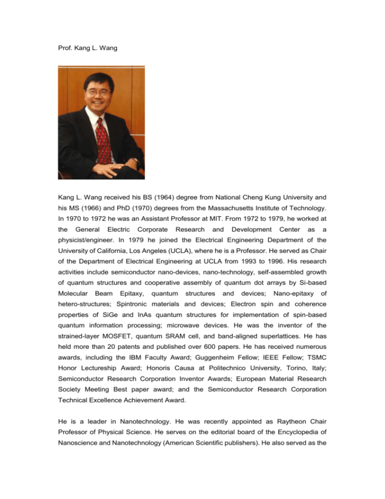
Prof. Kang L. Wang Kang L. Wang received his BS (1964) degree from National Cheng Kung University and his MS (1966) and PhD (1970) degrees from the Massachusetts Institute of Technology. In 1970 to 1972 he was an Assistant Professor at MIT. From 1972 to 1979, he worked at the General Electric Corporate Research and Development Center as a physicist/engineer. In 1979 he joined the Electrical Engineering Department of the University of California, Los Angeles (UCLA), where he is a Professor. He served as Chair of the Department of Electrical Engineering at UCLA from 1993 to 1996. His research activities include semiconductor nano-devices, nano-technology, self-assembled growth of quantum structures and cooperative assembly of quantum dot arrays by Si-based Molecular Beam Epitaxy, quantum structures and devices; Nano-epitaxy of hetero-structures; Spintronic materials and devices; Electron spin and coherence properties of SiGe and InAs quantum structures for implementation of spin-based quantum information processing; microwave devices. He was the inventor of the strained-layer MOSFET, quantum SRAM cell, and band-aligned superlattices. He has held more than 20 patents and published over 600 papers. He has received numerous awards, including the IBM Faculty Award; Guggenheim Fellow; IEEE Fellow; TSMC Honor Lectureship Award; Honoris Causa at Politechnico University, Torino, Italy; Semiconductor Research Corporation Inventor Awards; European Material Research Society Meeting Best paper award; and the Semiconductor Research Corporation Technical Excellence Achievement Award. He is a leader in Nanotechnology. He was recently appointed as Raytheon Chair Professor of Physical Science. He serves on the editorial board of the Encyclopedia of Nanoscience and Nanotechnology (American Scientific publishers). He also served as the Director of Marco Focus Center on Functional Engineered Nano Architectonics (FENA), an interdisciplinary Research Center, funded by the Semiconductor Industry Association and the Department of Defense to address the need of information processing technology beyond scaled CMOS. The Center involved 12 universities across the nation with 35 participating faculty members. He was also named the Director of Western Institute of Nanoelectronics (WIN) – a coordinated multi-project Research Institute. WIN is funded by NRI, Intel and the State of California. The current on-going projects are aimed at spintronics for low-power applications. He was also the founding director of the Nanoelectronics Research Facility (NRF) at UCLA (established in 1989) providing the infrastructure to further research in nanotechnology. In addition to these technical leadership contributions, he has provided academic leadership in engineering education. He was also the Dean of Engineering from 2000 to 2002 at the Hong Kong University of Science and Technology.


