ACasimirchipthatexploitsthevacuumenergy
advertisement
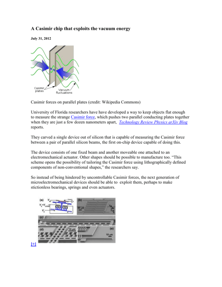
A Casimir chip that exploits the vacuum energy July 31, 2012 Casimir forces on parallel plates (credit: Wikipedia Commons) University of Florida researchers have have developed a way to keep objects flat enough to measure the strange Casimir force, which pushes two parallel conducting plates together when they are just a few dozen nanometers apart, Technology Review Physics arXiv Blog reports. They carved a single device out of silicon that is capable of measuring the Casimir force between a pair of parallel silicon beams, the first on-chip device capable of doing this. The device consists of one fixed beam and another moveable one attached to an electromechanical actuator. Other shapes should be possible to manufacture too. “This scheme opens the possibility of tailoring the Casimir force using lithographically defined components of non-conventional shapes,” the researchers say. So instead of being hindered by uncontrollable Casimir forces, the next generation of microelectromechanical devices should be able to exploit them, perhaps to make stictionless bearings, springs and even actuators. [+] The set-up of the experiment and device. (a) A simplified schematic (not to scale) of the beam, movable electrode and comb actuator supported by four springs, with electrical connections. The current amplifier provides a virtual ground to the right end of the beam. The suspended and anchored parts of the comb actuator are shown in dark and light colors respectively. The separation d between the beam and the movable electrode was controllably reduced so that the Casimir force can be detected. (b)-(e) Scanning electron micrographs of the entire micromechanical structure (b) and close-ups of: the doubly clamped beam (c), zoomed into the white dashed box in (b); the comb actuator (d) and the serpentine spring (e). (Credit: J. Zou, et al.) [+] Verios (credit: FEI) Microscopes for viewing nanoscale devices Monitoring these kind of ultra-small nanoscale devices requires special microscopes, such as the scanning electron microscope (SEM), which images a sample by scanning it with a beam of electrons. (The Casimir device image above is an example of an SEM image). An SEM can produce very high-resolution images of a sample surface, revealing details less than 1 nanometer in size (the size of small biomolecules). FEI has just announced the new Verios XHR SEM, which provides the sub-nanometer resolution and enhanced contrast needed for precise measurements in materials science and advanced semiconductor manufacturing applications. An even higher-resolution microscope is the transmission electron microscope (TEM), with a resolution of 0.5 Angstroms (.05 nm). An example of a TEM image is shown in this news item today on graphene layers. Another type of nanoscale microscope is the atomic force microscope (AFM). It has several advantages over the 2D SEM; it provides a 3D surface profile, for example. It also has disadvantages: it doesn’t allow for large scanned images, and is very slow, for example. Nonetheless, AFMs are vital tools in nanotechology, and nanoHUB.org has just announced a two-part, web-based course covering the principles and practice of atomic force microscopy.
