Solid State Physics MCQ Question Bank
advertisement
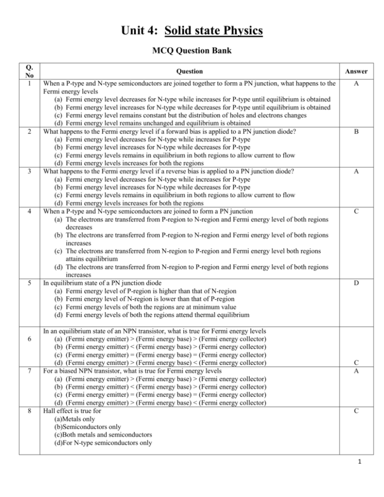
Unit 4: Solid state Physics MCQ Question Bank Q. No 1 2 3 4 5 6 7 8 Question Answer When a P-type and N-type semiconductors are joined together to form a PN junction, what happens to the Fermi energy levels (a) Fermi energy level decreases for N-type while increases for P-type until equilibrium is obtained (b) Fermi energy level increases for N-type while decreases for P-type until equilibrium is obtained (c) Fermi energy level remains constant but the distribution of holes and electrons changes (d) Fermi energy level remains unchanged and equilibrium is obtained What happens to the Fermi energy level if a forward bias is applied to a PN junction diode? (a) Fermi energy level decreases for N-type while increases for P-type (b) Fermi energy level increases for N-type while decreases for P-type (c) Fermi energy levels remains in equilibrium in both regions to allow current to flow (d) Fermi energy levels increases for both the regions What happens to the Fermi energy level if a reverse bias is applied to a PN junction diode? (a) Fermi energy level decreases for N-type while increases for P-type (b) Fermi energy level increases for N-type while decreases for P-type (c) Fermi energy levels remains in equilibrium in both regions to allow current to flow (d) Fermi energy levels increases for both the regions When a P-type and N-type semiconductors are joined to form a PN junction (a) The electrons are transferred from P-region to N-region and Fermi energy level of both regions decreases (b) The electrons are transferred from P-region to N-region and Fermi energy level of both regions increases (c) The electrons are transferred from N-region to P-region and Fermi energy level both regions attains equilibrium (d) The electrons are transferred from N-region to P-region and Fermi energy level of both regions increases In equilibrium state of a PN junction diode (a) Fermi energy level of P-region is higher than that of N-region (b) Fermi energy level of N-region is lower than that of P-region (c) Fermi energy levels of both the regions are at minimum value (d) Fermi energy levels of both the regions attend thermal equilibrium A In an equilibrium state of an NPN transistor, what is true for Fermi energy levels (a) (Fermi energy emitter) > (Fermi energy base) > (Fermi energy collector) (b) (Fermi energy emitter) < (Fermi energy base) > (Fermi energy collector) (c) (Fermi energy emitter) = (Fermi energy base) = (Fermi energy collector) (d) (Fermi energy emitter) > (Fermi energy base) < (Fermi energy collector) For a biased NPN transistor, what is true for Fermi energy levels (a) (Fermi energy emitter) > (Fermi energy base) > (Fermi energy collector) (b) (Fermi energy emitter) < (Fermi energy base) > (Fermi energy collector) (c) (Fermi energy emitter) = (Fermi energy base) = (Fermi energy collector) (d) (Fermi energy emitter) > (Fermi energy base) < (Fermi energy collector) Hall effect is true for (a)Metals only (b)Semiconductors only (c)Both metals and semiconductors (d)For N-type semiconductors only B A C D C A C 1 9 10 11 12 13 14 15 16 17 18 Hall effect is true for (a) Both N-type and P-type semiconductors (b) N-type Semiconductors only (c) P-type Semiconductors only (d) Metals only When current flows along the length of the semiconductor slab and magnetic field applied is perpendicular the length to Hall voltage developed is (a) Along the length (b) Along the thickness (c) Along the width (d) Along the edges from where current enters In Hall effect, if only the direction of the current is changed in the material (a) The value of Hall voltage developed increases (b) The value of Hall voltage developed in opposite direction, but its value remains constant (c) The value of Hall voltage developed decreases (d) The Hall effect do not appear In Hall effect, if only the direction of the magnetic field applied to the material is changed (a)The value of Hall voltage appears (b)The value of Hall voltage developed decreases (c)The value of Hall voltage developed in opposite direction, but its value remains constant (d)The Hall effect do not appear A In Hall effect, if only the direction of the current is changed in the material the Hall electric field (a) Hall electric field is developed in opposite direction (b) Hall electric field do not change the direction (c) Hall electric field increases (d) Hall electric field decreases If the thickness of the material is reduced, the Hall voltage developed (a) Decreases (b) Increases (c) Remains constant (d) Changes the direction If the thickness of the material is increased, the Hall voltage developed (a) Decreases (b) Increases (c) Remains constant (d) Changes the direction If the strength of magnetic field is increased, the Hall voltage developed (a) Decreases (b) Remains constant (c) Increases (d) Changes the direction If the strength of magnetic field is decreased, the Hall voltage developed (a) Decreases (b) Increases (c) Remains constant (d) Changes the direction If the magnitude of current is increased, the Hall voltage developed (a) Decreases (b) Increases (c) Remains constant (d) Changes the direction A C B C B A C A B 2 19 If the magnitude of current is decreased, the Hall voltage developed (a)Decreases (b)Increases (c)Remains constant (d)Changes the direction A 20 If the density of charge carriers is increased, the value of Hall voltage (a) Decreases (b) Increases (c) Remains constant (d) Changes the direction Which of the following statements correctly describes a metal within band theory? A 21 22 23 24 25 26 28 29 C (a) A material possessing moderate band gap (b) A material possesses a large band gap (c) A material with zero band gap (d) A material with infinite band gap Which is the correct ordering of the band gaps energy? (a) Diamond > silicon > copper (b) Diamond < silicon < copper (c) Diamond < silicon > copper (d) Diamond < silicon < copper Which statement is true regarding electrical conductivity of materials? (a) Electrical conductivity of a metal increases with temperature (b) Electrical conductivity of a semiconductor increases with temperature (c) Electrical conductivity of a metal decreases with temperature (d) Electrical conductivity of a semiconductor decreases with temperature Which statement is incorrect at ordinary room temperature? (a) In metals electron can jump from valence band to conduction band easily (b) In semiconductors few electrons can jump from valence band to conduction band (c) In semiconductors is pure insulator at ordinary room temperature (d) In insulators electrons cannot jump from valence band to conduction band Which statement is incorrect about semiconductors? (a) A charge carrier may be either a positive hole or an electron (b) Ga-doped Si is a p-type semiconductor (c) n- and p-type semiconductors are intrinsic semiconductors (d) Doping Si with As introduces a donor level below the conduction band At 0 Kelvin, semiconductors are (a) Perfect metals (b) Perfect semiconductors (c) Perfect non-metals (d) Perfect insulator Solids with high value of conductivity are called: (a) Conductors (b) Non-metal (c) Insulator (d) Semi conductor The electrons in valence band are (a) Freely moving inside the solid (b) Tightly bonded inside the solid (c) Lies in the innermost orbits and cannot be made free (d) Lies in the outermost orbits and cannot be made free A B C C D A A 3 30 31 32 33 34 35 36 37 38 39 40 At absolute zero (0 K) conduction band will be (a) Fully occupied by electrons (b) Completely empty (c) Partially occupied by electrons (d) Partially occupied by holes Above absolute zero, what is true for metals? (a) Conduction band is always empty (b) Valence band is always empty (c) Conduction band is partially occupied (d) Valence band is always full For metals conduction band and valence band are (a) Fully occupied (b) Empty (c) Partially occupied (d) Overlapping For a metal which is the incorrect statement? (a) Electrons are freely moving in the solid and have energy greater than valence electrons (b) Electrons can remain simultaneously in conduction band and valence band (c) Electrons in valence band may have energy equal to conduction band (d) Electrons in valence band cannot have energy equal to conduction band What is the correct statement for an insulator? (a) The band gap energy is very high (b) The conduction band and valence cannot overlap (c) The conduction band and valence band may overlap (d) The conduction band and valence cannot have very little difference of energy Pure silicon at 0 K is an (a) Intrinsic semiconductor (b) Extrinsic semiconductor. (c) Metal (d) Insulator The energy required to break a covalent bond in a semiconductor (a) is equal to 1 eV (b) is equal to the width of the forbidden gap (c) is greater in Ge than in Si (d) is the same in Ge and Si As electrons in conduction band have high energy, where is their location in solids? (a) Always near the top of the crystal (b) Always at the surface of the crystal (c) Anywhere in the solid moving freely (d) Always bound to its parent atom in outermost orbit At 0 K, all the valence electrons in an intrinsic semiconductor (a) are in the valence band (b) are in the forbidden gap (c) are in the conduction band (d) are free electrons P-type and N-type extrinsic semiconductors are formed by adding impurities of valency? (a) 5 and 3 respectively. (b) 5 and 4 respectively. (c) 3 and 5 respectively. (d) 3 and 4 respectively. In an insulator, the forbidden energy gap is of the order of (a) 1 MeV (b) 0.1 MeV (c) eV (d) 5eV Q. No D D B D B C A C D 4 41 42 43 44 45 46 47 48 49 50 At 0 K temperature, a p-type semiconductor (a) Does not have any charge carriers (b) Has few electrons and few free holes (c) Has few holes but no electrons (d) Has equal number of holes and electrons The bond that exists in a semiconductor is (a) Ionic bond (b) Covalent bond (c) Metallic bond (d) Hydrogen bond A pure semiconductor behaves slightly as a conductor at (a) Only at very high temperatures (b) Only above room temperature (c) At any energy above 0 K (d) Only at room temperature Fermi level for a metal is (a)Highest energy level occupied by electrons at 0 0C (b)Average value of all available energy levels (c)Highest energy level occupied by electrons at 0 K (d )Addition of energy of all available electron energy levels Fermi level for an intrinsic semiconductor is (a) Highest energy level occupied by electrons at 0 0C (b) Average value of all available energy levels (c) Highest energy level occupied by electrons at 0 K (d) Reference energy level at the centre of the forbidden energy gap What is the position of Fermi level in an n-type semiconductor? (a) In between energy levels of conduction band and donor atoms (b) In between energy levels of donor atoms and Fermi energy levels (c) In between energy levels of valence band and Fermi level (d) Close to the valence band The Fermi Function represents the probability of occupation which of the following energy level by an electron? (a) For electrons only at Fermi energy level (b) For electrons at any energy level (c) For electrons only above Fermi energy level (d) For electrons only below Fermi energy level Fermi level represents the energy level with probability of its occupation of (a) 0 % (b) 25 % (c) 50 % (d) 100 % The probability of occupancy of electrons above Fermi level at T=0°K is (a) 0 % (b) 25% (c) 50% (d) 100% The probability of occupancy of electrons below Fermi level at T=0°K is (a) 0 % (b) 25% (c) 50% (d) 100% A B C A D B B C A D 5 51 55 The energy level of a donor atom typically lies very close to (a) Just above the conduction band (b) just below the conduction band (c) just above the valence band (d) just below the valence band The energy level of a acceptor atom typically lies very close to (a) just above the conduction band (b) just below the conduction band (c) just above the valence band (d) just below the valence band Due to the addition of a donor atom the original Fermi energy level in an intrinsic semiconductor (a) moves toward conduction band (b) moves toward valence band (c) remains at the centre of the forbidden energy gap (d) is not affected Due to the addition of an acceptor atom the original Fermi energy level in an intrinsic semiconductor (a) moves toward conduction band (b) moves toward valence band (c) remains at the centre of the forbidden energy gap (d) is not affected The free electron theory could not explain which of the following properties? 56 (a) Electrical and thermal conductivity of metals (b) Thermal and thermal conductivity of non-metal (c) Ferromagnetism (d) Ohm’s law Free electron theory is based on which of the following assumption? 52 53 54 (a) (b) (c) (d) 57 58 59 B C B B A Conductivity almost remain constant with only little heating Conductivity increases along with little heating of the material Conductivity decreases along with little heating of the material Conductivity decreases as electrons are emitted from the material When light incidents on semiconductors what is the effect on its conductivity? (a) (b) (c) (d) A Conductivity of metals increases with increase in temperature Conductivity of metals decreases with increase in temperature Conductivity of semiconductors decreases with increase in temperature Conductivity of semiconductors do not change with increase in temperature When light incidents on metals what is the effect on its conductivity? (a) (b) (c) (d) C Electrons are freely moving only at the centre of the solid Electrons behaves are freely moving through entire the solid Electrons can move freely only at the top surface of the solid Electrons can move freely only along the surfaces of the solid Which statement is correct regarding the influence of temperature on conductivity? (a) (b) (c) (d) B D Conductivity almost remain constant with little heating Conductivity is not affected Conductivity increases as electrons are promoted to conduction band after absorbing light Conductivity decreases as electrons absorb photons and move with more random motion 6 60 What is the effect of impurity on metals? (a) (b) (c) (d) 61 62 C Number of available energy levels of electrons in unit volume per unit temperature Number of available energy levels of electrons in unit volume Number of available energy levels of electrons in unit volume per unit energy interval Number of available electrons of per unit volume of the solid Under the influence of external electric or magnetic field, when an electrons moves inside a solid what happens to its mass? (a) (b) (c) (d) 63 Impurity increases into increase of mobility of electrons Impurity result into more scattering of electrons and conductivity decreases Impurity result into more scattering of electrons and conductivity increases Impurity does not affect the conductivity Density of states function implies (a) (b) (c) (d) B C The mass of electron is a constant quantity and it remains constant The mass of electron increases due to absorption of external energy The mass of electron increases or decreases depending on the potential of positive ions The external field will only change the resistance, but mass of electron is not affected What is the effect of at very high temperature on N-type semiconductors? A (a) Concentration of electrons and holes is almost equal due to ionization of donor ions and it turns into intrinsic semiconductor (b) Concentration of electrons is more and it becomes more negative (c) More holes are created as electrons become free and it turns into P-type semiconductor (d) It turns more negative as more electrons will break the bonds and become free 64 What is the effect of at very high temperature on P-type semiconductors? A (a) Concentration of electrons and holes is almost equal due to ionization of donor ions and it turns into intrinsic semiconductor (b) Concentration of holes is more and it becomes more positive (c) More electrons are created and it turns into N-type semiconductor (d) It turns more positive as more electrons will break the bonds and more holes are created 65 What is the effect of very high temperature on N-type semiconductors? (a) (b) (c) (d) 67 Fermi level continue to increases as more electrons are free and conducting Fermi level continue to decreases as more electrons are free creating more holes Fermi level becomes equal to its intrinsic Fermi level is concentration of holes and electrons is balanced Fermi level is unbalanced and fluctuates rapidly If the doping concentration of donor ions increased, what is the effect on Fermi energy of N-type semiconductor? (a) (b) (c) (d) C B Fermi level increase but always remain below the energy level of conduction band Fermi level increases and merge into energy level of conduction band Fermi level increase and goes above the energy level of conduction band Fermi level is unbalanced and fluctuates rapidly 7 68 If the doping concentration of acceptor ions increased, what is the effect on Fermi energy of P-type semiconductor? (a) (b) (c) (d) 69 70 72 73 74 C ne >> nh ne > nh nh >> ne nh > ne The Fermi level in an n-type semiconductor at 00 K lies (a) (b) (c) (d) B Along opposite edges of its thickness Along opposite edges of its width Along opposite edges of its length Along the ends from where current enters For silicon doped with trivalent impurity, (a) (b) (c) (d) A Decreases Increases Remains constant Changes the direction If the current flowing through the semiconductor slab along its length, Hall voltage and electric field developed is due to accumulation of charge carriers (a) (b) (c) (d) D Diffusion is caused because of random movement of electrons and holes within the solid Diffusion is caused due removal of electrons in solid when power supply is connected Diffusion is passing of electrons and holes through potential barrier Diffusion is caused because of unbalanced distribution of concentration of electrons or holes within the solid If the density of charge carriers is increased, the value of Hall coefficient (a) (b) (c) (d) D Drift current is caused because of unequal concentration of electrons within the solid Drift current is caused because of unequal concentration of holes within the solid Drift current is caused due to smooth flow of electrons within the solid Drift current is caused because of random motion of electrons with ions or electrons What is true regarding diffusion? (a) (b) (c) (d) 71 Fermi level decreases but always remain above the energy level of valence band Fermi level decreases and merge into energy level of valence band Fermi level decreases increase and goes down the energy level of valence band Fermi level is unbalanced and fluctuates rapidly What is true regarding drift current? (a) (b) (c) (d) B B Below the donor level. Half way between the bottom of conduction band and donor level. Exactly in the middle of hand gap. Half way between the top of valence band and the acceptor level. 8 75 If the Fermi energy of silver at 00 K is 5 electron volt, the mean energy of electron in silver at 00 K is (a) (b) (c) (d) 76 6 electron volt. 12 electron volt. 1.5 electron volt. 3 electron volt. The probability of occupation of an energy level E, when E – EF = kT, is given by (a) (b) (c) (d) D D 0.73 0.63 0.5 0.27 77 Which of the following elements is a covalently bonded crystal? (a) aluminium (b) sodium chloride (c) germanium (d) lead C 78 The Fermi level is (a) an average value of all available energy levels. (b) an energy level at the top of the valence band. (c) the highest occupied energy level at 0 0c. (d) the highest occupied energy level at 0 0k. D 79 Mobility of electron is C (a) (b) (c) (d) Average flow of electrons per unit field. Average applied field per unit drift velocity. Average drift velocity per unit field. Reciprocal of conductivity per unit charge. 80 Fermi level represents the energy level with probability of its occupation of C 81 (a) 0 %. (b) 25 %. (c) 50 %. (d) 100 %. Hall effect can be used to measure D 82 (a) mobility of semiconductors. (b) conductivity of semiconductors. (c) resistivity of semiconductors. (d) all of these The energy required to break a covalent bond in a semiconductor B (a) (b) (c) (d) is equal to 1 eV is equal to the width of the forbidden gap is greater in Ge than in Si is the same in Ge and Si 9 83 At absolute zero temperature, the probability of finding an electron at an energy level E is zero when (a) (b) (c) (d) 84 85 87 C A/cm2 mho/meter cm2/V.s V/cm Energy band gap size for semiconductors is in the range ________ eV. (a) (b) (c) (d) A 10-10(Ω-mm)-1 10-10(Ω-cm)-1 10-10(Ω-m)-1 10-8(Ω-m)-1 Units for electric field strength (a) (b) (c) (d) 86 E < EF E > Ef 2E E = f None Electrical conductivity of insulators is in the range of _______. (a) (b) (c) (d) B B 1-2 2-3 3-4 >4 Energy band gap size for insulators is in the range ________ eV. D 88 (a) 1-2 (b) 2-3 (c) 3-4 (d) > 4 Flow of electrons is affected by the following D 89 (a) Thermal vibrations (b) Impurity atoms (c) Crystal defects (d) all Flow of electrons is affected by the following D (a) (b) (c) (d) 90 Thermal vibrations Impurity atoms Crystal defects All Fermi energy level for p-type extrinsic semiconductors lies (a) (b) (c) (d) B At middle of the band gap Close to conduction band Close to valence band None 10 91 Fermi energy level for n-type extrinsic semiconductors lies B 92 (a) At middle of the band gap (b) Close to conduction band (c) Close to valence band (d) None Fermi energy level for intrinsic semiconductors lies C (a) At middle of the band gap (b) Close to conduction band (c) Close to valence band (d) None Not an example for intrinsic semiconductor A (a) Si (b) Al (c) Ge (d) Sn In intrinsic semiconductors, number of electrons __________ number of holes. C (a) Equal (b) Greater than (c) Less than (d) Can not define In p-type semiconductors, number of holes __________ number of electrons. A 96 (a) Equal (b) Greater than (c) Less than (d) Twice Mobility of holes is ___________ mobility of electrons in intrinsic semiconductors. D 97 (a) Equal (b) Greater than (c) Less than (d) Can not define Fermi level for extrinsic semiconductor depends on D 98 (a) Donor element (b) Impurity concentration (c) Temperature (d) All To measure light intensity we use C 99 (a) LED with forward bias (b) LED with reverse bias (c) photodiode with reverse bias (d) photodiode with forward bias In integrated circuits, npn construction is preferred to pnp construction because B 93 94 95 (a) (b) (c) (d) npn construction is cheaper to reduce diffusion constant, n-type collector is preferred npn construction permits higher packing of elements p-type base is preferred 11 100 101 102 103 The photoelectric work function of a surface is 2.2 eV. The maximum kinetic energy of photo electrons emitted when light of wave length 6200 A.U. is incident on the surface is (a) 1.6 eV (b) 1.4 eV (c) 1.2 eV (d) Photo electrons are not emitted A metallic surface is irradiated by monochromatic light of frequency ν1and stopping potential is found to be V1. If light of frequency ν2 irradiates the surface, the stopping potential will be (a) (a) V1 + (h/e) (ν1 + ν2) (b) V1 + (h/e) (ν2 – ν1) (c) V1 + (e/h) (ν2 – ν1) (d) V1 - (h/e) (ν1 + ν2) The retarding potential required to stop the emission of photoelectrons when a photosensitive material of work function 1.2 eV is irradiated with ultraviolet rays of wave length 2000 A.U. is (a) 4V (b) 5V (c) 6V (d) 8V The photoelectric effect is __________. (a) (b) (c) (d) 104 105 106 107 D B B D a relativistic effect the production of current by silicon solar cells when exposed to sunlight the total reflection of light by metals giving them their typical luster the ejection of electrons by a metal when struck by lightens Substances which allow electric current to pass through them are called (a) Conductors (b) insulation (c) semi conductors (d) none of the above A copper wire of length l and diameter d has potential difference V applied at its two ends. The drift velocity is vd. If the diameter of wire is made d/3, then drift velocity becomes (a) 9 vd (b) vd / 9 (c) vd /3 (d) vd. The unit of electrical conductivity is (a) mho / metre (b) mho / sq. m (c) ohm / metre (d) ohm / sq. m. All good conductors have high (a) resistance (b) electrical conductivity (c) electrical and thermal conductivity (d) conductance. A D A D 12 108 A silicon sample is uniformly doped with 1016 phosphorus atoms/cm3 and 2 × 10¹⁶ boron atoms/cm3. If all the dopants are fully ionized, the material is: B 109 (a) n-type with carrier concentration of 3 × 10¹⁶/cm3 (b) p-type with carrier concentration of 1016/cm3A (c) p-type with carrier concentration of 4 × 10¹⁶/cm3 (d) Intrinsic Measurement of Hall coefficient enables the determination of: B 110 (a) Mobility of charge carriers (b) Type of conductivity and concentration of charge carriers (c) Temperature coefficient and thermal conductivity (d) None of the above The probability that an electron in a metal occupies the Fermi-level, at any temperature (>0 K) is: C 111 (a) 0 (b) 1 (c) 0.5 (d) None of these the conductivity of an intrinsic semiconductor is given by (symbols have the usual meanings): C 112 113 114 (a) σi = eni2 (µn – µp) (b) σi = eni (µn – µp) (c) σi = eni (µn + µp) (d) none of the above The Hall coefficient of sample (A) of a semiconductor is measured at room temperature. The Hall coefficient of (A) at room temperature is 4×10⁻⁴ m3 coulomb–1. The carrier concentration in sample A at room temperature is: (a) ~ 1021 m–3 (b) ~ 1020 m–3 (c) ~ 1022 m–3 (d) None of the above If the drift velocity of holes under a field gradient of 100v/m is 5m/s, the mobility (in the same SI units) is (a) 0.05 (b) 0.55 (c) 500 (d) 50 The Hall Effect voltage in intrinsic silicon is: (a) (b) (c) (d) C A C Positive Zero Negative None of the above 13 115 The Hall coefficient of an intrinsic semiconductor is: B 116 (a) Positive under all conditions (b) Negative under all conditions (c) Zero under all conditions (d) None of the above Consider the following statements: pure germanium and pure silicon are examples of: A 1. Direct band-gap semiconductors 2. Indirect band-gap semiconductors 3. Degenerate semiconductors which of these statements are true 117 118 119 120 (a) 1 alone is correct (b) 2 alone is correct (c) 3 alone is correct (d) None of the above When ne and nh are electron and hole densities, and µe and µn are the carrier mobilities, the Hall coefficient is positive when (a) nh µh > neµe (b) nh µh2 > neµe2 (c) nhµh < neµh (d) None of the above The electron and hole concentrations in a intrinsic semiconductor are ni and pi respectively. When doped with a p-type material, these change to n and p, respectively. Then: (a) n + p = ni + pi (b) n + ni = p + pi (c) np = nipi (d) None of the above If the temperature of an extrinsic semiconductor is increased so that the intrinsic carrier concentration is doubled, then: (a) The majority carrier density doubles (b) The minority carrier density doubles (c) Both majority and minority carrier densities double (d) None of the above The mobility is given by (notations have their usual meaning): (a) (b) (c) (d) 122 C C A µ = V0/E0 µ = V02/E0 µ = V0/E02 None of the above The intrinsic carrier density at 300K is 1.5 x 10¹⁰/cm3 in silicon. For n-type silicon doped to 2.25 x 10¹⁵ atoms/cm3, the equilibrium electron and hole densities are: (a) (b) (c) (d) B D n0 = 1.5 x 10¹⁶/cm3, p0 = 1.5 x 10¹²/cm3 n0 = 1.5 x 10¹⁰/cm3, p0 = 2.25 x 10¹⁵/cm3 n0 = 2.25 x 10¹⁷/cm3, p0 = 1.0 x 10¹⁴/cm3 None of the above 14 123 In a p-type silicon sample, the hole concentration is 2.25 x 10¹⁵/cm3. If the intrinsic carrier concentration 1.5 x 10¹⁰/cm3, the electron concentration is (a) (b) (c) (d) D 1021/cm3 1010/cm3 1016/cm3 None of the above 15


![Intro to Semiconductors and Diodes []](http://s2.studylib.net/store/data/005340797_1-9cc5e13687b40f30b11ab4990fa74479-300x300.png)