Reed_Frankie_ProjectSummary
advertisement
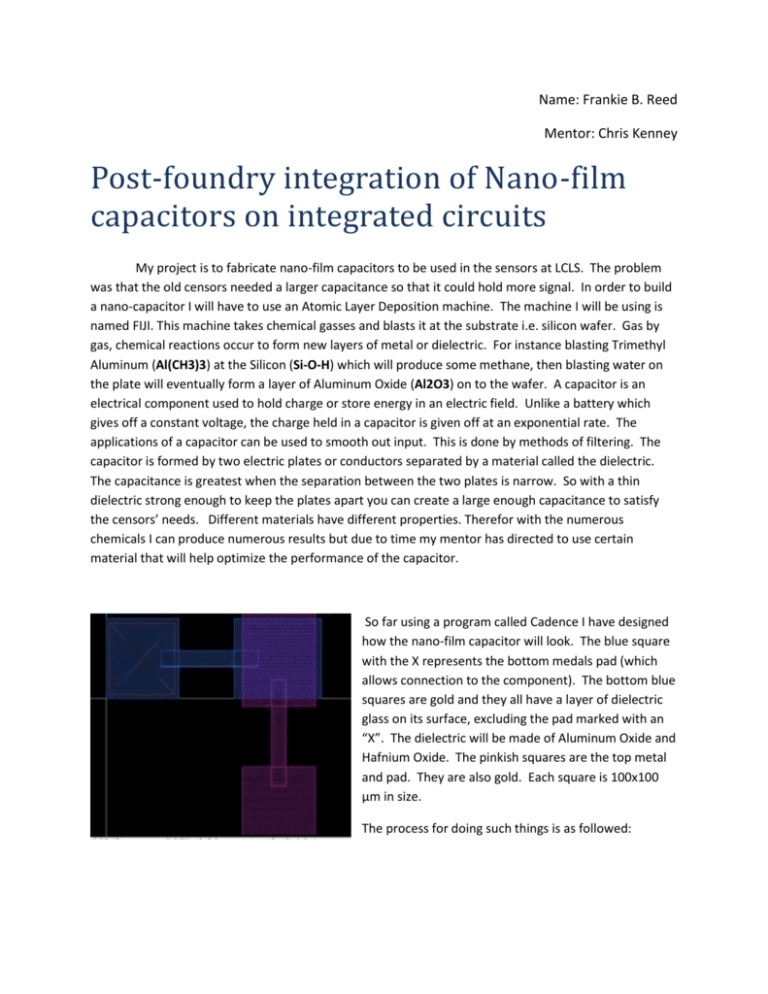
Name: Frankie B. Reed Mentor: Chris Kenney Post-foundry integration of Nano-film capacitors on integrated circuits My project is to fabricate nano-film capacitors to be used in the sensors at LCLS. The problem was that the old censors needed a larger capacitance so that it could hold more signal. In order to build a nano-capacitor I will have to use an Atomic Layer Deposition machine. The machine I will be using is named FIJI. This machine takes chemical gasses and blasts it at the substrate i.e. silicon wafer. Gas by gas, chemical reactions occur to form new layers of metal or dielectric. For instance blasting Trimethyl Aluminum (Al(CH3)3) at the Silicon (Si-O-H) which will produce some methane, then blasting water on the plate will eventually form a layer of Aluminum Oxide (Al2O3) on to the wafer. A capacitor is an electrical component used to hold charge or store energy in an electric field. Unlike a battery which gives off a constant voltage, the charge held in a capacitor is given off at an exponential rate. The applications of a capacitor can be used to smooth out input. This is done by methods of filtering. The capacitor is formed by two electric plates or conductors separated by a material called the dielectric. The capacitance is greatest when the separation between the two plates is narrow. So with a thin dielectric strong enough to keep the plates apart you can create a large enough capacitance to satisfy the censors’ needs. Different materials have different properties. Therefor with the numerous chemicals I can produce numerous results but due to time my mentor has directed to use certain material that will help optimize the performance of the capacitor. So far using a program called Cadence I have designed how the nano-film capacitor will look. The blue square with the X represents the bottom medals pad (which allows connection to the component). The bottom blue squares are gold and they all have a layer of dielectric glass on its surface, excluding the pad marked with an “X”. The dielectric will be made of Aluminum Oxide and Hafnium Oxide. The pinkish squares are the top metal and pad. They are also gold. Each square is 100x100 μm in size. The process for doing such things is as followed: 1) Start 12 wafers 6) Spin coat SPR3612 1.0 um 2) WBNONMETAL clean 7) KS or EV 3) WBDIFF clean 8) SVGDEV 4) Grow 4000A thermal oxide WET1000 1:30:00 9) Innotec Deposit Ti (50A) Au (200A) 5) WBNONMETAL 10) Soak acetone overnight 11) Ultrasonic liftoff 12) Clean 18) Spin coat SPR3612 1.0 um 13) ALD 100 A of AlO3, HfO2 19) KS or EV 14) Spin coat SPR3612 1.0 um 20) SVGDEV 15) KS or EVSVGDEV 21) Aluminum etch at WBGENERAL 16) Etch dielectric (PAD ETCH or DRYTEK2 GOLD) 22) Clean 17) Innotec 4000 A Aluminum Nano-Resistor I was also given the task to make a nano-resistor. This resistor is as shown below. The calculated resistance is said to be 1000 ohms. This resistor may also used in the censor as well. The process for making the resistor is as follows. 1) Start 4 wafers 2) WBNONMETAL clean 3) WBDIFF clean 4) Grow 4000A thermal oxide WET1000 1:30:00 5) ALD Platinum 100A 6) Spin coat SPR3612 1.0 um 7) KS or EV 8) SVGDEV 9) Platinum etch A.R.
![Sample_hold[1]](http://s2.studylib.net/store/data/005360237_1-66a09447be9ffd6ace4f3f67c2fef5c7-300x300.png)
