Simulation_of_E-fields_in_GTO_stack
advertisement
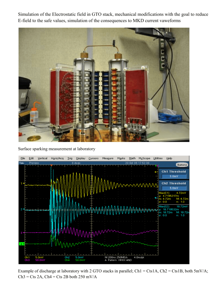
Simulation of the Electrostatic field in GTO stack, mechanical modifications with the goal to reduce E-field to the safe values, simulation of the consequences to MKD current vaweforms Surface sparking measurement at laboratory Example of discharge at laboratory with 2 GTO stacks in parallel; Ch1 = Cts1A, Ch2 = Cts1B, both 5mV/A; Ch3 = Cts 2A, Ch4 = Cts 2B both 250 mV/A Sparking between GTO deflector and surface of plexiglas isolator – plexiglas surface charging Corresponding Cts1ab and Cts2ab, Icts1Amax = 10 A, Icts2Amax= 600 mA, U = 29 kV GTO stacks with return bars withot plexiglas tude Sparking between GTO deflectors and silicon surface (plexiglas tube removed) even more intense – most likely due to lower surface and volumic resistance of silicon polymer compare to plexiglas Corresponding Cts1ab and Cts2ab, Icts1Amax = 13 A, Icts2Amax= 900 mA, U = 29 kV 2-D simulation of an electric field between upper GTO deflector smalest radius (1.5 mm!) and return metal rod with silicon rubber and plexiglass tube. For simplicity reson the small radius is parallel with metal rod. Emax > 7.8 MV/m! 2-D simulation of an electric field between upper GTO deflector (not taking into account small radius on deflector) and return metal rod with silicon rubber and plexiglass tube. Emax > 7.4 MV/m! 3-D simulation of electric field arround 2 uppermost GTO deflectors (smalest radius of 1.5 mm!) and return metal rod with silicon rubber and plexiglass tube. Emax ~ 8.1 MV/m! Situation after removal of plexiglass insulation of return metal rod (leaving silicon insulation) and a metal rod with insulation; Emax > 5.5 MV/m still too high leading to air ionisation One of possible solutions: reduction of the E-field intensity in the air by hybrid insulation: allowing accumulation of a surface charge on insulations of both conductors. Problem: initial surface charge deposition most likely by ionization of the air between insulators surfaces and hence resulting displacemnt current. Necessity to ensure high volumic and surface resistance of insulators to reduce frequency and intensity of microdischarges keeping surface charge on the limit of the air ionisation – might be not easy due to ambient humidity (and surface afinity to it) and dust deposition Stack return bars (original) displaced by 5 mm form actual position, insulation on the surface of the original GTO deflectors; Emax > 2.7 MV/m; value higher than air ionisation limit Stack return bars (original) displaced by 7.5 mm form actual position, insulation on the surface of the original GTO deflectors; Emax > 2.3 MV/m; value close to the of the air ionisation limit Stack return bars (original) displaced by 10 mm form actual position, insulation on the surface of the original GTO deflectors; Emax ~ 2 MV/m; sufficiently low to avoid air ionisation Stack return bars displaced by 5 mm form actual position, GTO deflector diameter reduced to 104 mm (from actual 107.5 mm); Emax > 2.4 MV/m; value close to the air ionisation limit Stack return bars displaced by 8 mm form actual position, GTO deflector diameter reduced to 104 mm (from actual 107.5 mm); Emax ~ 2 MV/m; safe value! Situation with original return rods and with original but screened GTO deflectors; Corner effect is clearly removed but field is still too high Emax > 4.7 MV/m; solution is usable only with accepting the surface charging effect. Situation with actual return rods moved by 8 mm away from actual position and with screened original GTO deflectors; Emax ~ 2.26 MV/m; solution is probably acceptable but increases the stack inductance. Situation with actual return rods moved by 10 mm away from actual position and with screened original GTO deflectors; Emax < 2 MV/m; solution is acceptable but increases the stack inductance. Stack return bars displaced by 8 mm form actual position, GTO deflector diameter reduced to 104 mm (from actual 107.5 mm); Emax < 2 MV/m; safe value! 6 mm metal rod + 2 mm silicon (ε=3) + 5 mm teflon tube (ε=2.1); GTO deflector outer radius reduced to 100 mm (GTO dimensions) with 2 mm araldite coaling (ε=4.8); Emax ~ 2.25 MV/m 6 mm metal rod + 2 mm silicon (ε=3) + 5 mm teflon tube (ε=2.1); GTO deflector outer radius reduced to 100 mm (GTO dimensions) with 2 mm araldite coaling (ε=4.8); Emax ~ 2.2 MV/m Actual situation; Emax ~ 8.1 MV/m! Solution I.: Modified metal returned rod (diam 6 mm + 2mm silicon + 5 mm teflon) in actual position, modified GTO deflectors (100 mm instead of actual 107.5 mm); Emax ~ 2.2 MV/m Solution II.: Original metal rods but moved 8 mm away from GTO deflectors; modified GTO deflectors (104 mm instead of actual 107.5 mm); Emax < 2 MV/m Solution III.: Original metal rods (with silicon and plexiglass) moved 8 mm away from GTO deflectors; insulated original GTO deflectors; Emax ~ 2.26 MV/m Magnetic flux density at I = 1A for actual situation; Corresponding GTO stack inductance L = 132 nH (at 100 kHz). Magnetic flux density at I = 1A for solution I.: Metal rod diameter reduced to 6 mm, kept position relative to GTO; Corresponding GTO stack inductance L = 152 nH. Magnetic flux density at I = 1A for solution II.: Metal rod displaced by 8 mm further relative to GTO; Corresponding GTO stack inductance L = 146 nH. 18.91KA 18.90KA Diff. Tovershot1 = + 6.7 ns Diff. Iovershot1 = - 20 A (-0.11%) 18.88KA 18.87KA 4.46us 4.48us 4.50us 4.51us -I(L9) Time Influence of GTO stack inductance to MKD current waveform; Actual stack with inductance of 132 nH (red) and modified one with inductance of 146nH (green); MKD supply voltage of 29 092 V (7 Tev); Overshot1 value differs by - 0.11% and is delayed by + 7 ns for modified stack. Solution: increasing of the MKD voltage by 0.1%: 18.91KA 18.90KA Tovershot1 = 4.485 us Iovershot1 = 18.899 kA 18.88KA 18.87KA 4.46us -I(L9) 4.48us 4.50us 4.51us Time MKD supply voltage increased to 29 121 V (+0.1%); Modified GTO stack with increased inductance (146 nH) used; Iovershot1 = 18.899 kA, Tovershot1 = 4.485 us 17.93KA 17.92KA Diff. Tref 100% = -3 ns Diff. Iref 100% = - 18 A ( -0.1%) 17.90KA 17.89KA 9.36us 9.40us 9.45us 9.50us -I(L9) Time Influence of GTO stack inductance to MKD current waveform; Actual stack with inductance of 132 nH (red) and modified one with inductance of 146nH (green). Iref 100 % value differs by - 0.1% and is advanced by 3ns for modified stack. 17.93KA 17.92KA Tref 100% = 9.426 us Iref 100% = 17.916 kA 17.90KA 17.89KA 9.36us -I(L9) 9.40us 9.45us 9.50us Time MKD supply voltage increased to 29 121 V (+0.1%); Modified GTO stack with increased inductance (146 nH) used; I ref 100% = 17.916 kA, Tref 100% = 9.426 us 36.0A Ttreshold = 1.061 us 35.9A Diff. Ttreshold = + 44 ps 35.8A 35.7A 35.6A 1.06125us -I(L9) 1.06140us 1.06160us 1.06175us Time Rise time to Itreshold (35.8 A) difference due to increased stack inductance ~ +44 ps, Actual stack with inductance of 132 nH (red) and modified one with inductance of 146nH (green) 36.0A Itreshold = 35.8 A 35.9A Ttreshold = 1.061 us 35.8A 35.7A 35.6A 1.06125us -I(L9) 1.06140us 1.06160us 1.06175us Time MKD supply voltage increased to 29 121 V (+0.1%); Modified GTO stack with increased inductance (146 nH) used; I treshold = 35.8 A, Ttreshold = 1.061 us 17.93KA Diff. in Time to reach Iref 100% = + 0.6 ns 17.92KA 17.90KA 17.89KA 3.780us 3.782us 3.784us 3.786us -I(L9) Time Difference in Tdelay (time to reach Iref 100% for the first time) between actual stack (red; Iref100% = 17.9155kA) and modified one (green; Iref100% = 17.898 kA) is + 0.6 ns; Trise value is hence 2.72 us and 2.73 us respectively; 17.93KA Tdelay = 3.784 us 17.92KA 17.90KA 17.89KA 3.780us -I(L9) 3.782us 3.784us 3.786us Time MKD supply voltage increased to 29 121 V (+0.1%); Modified GTO stack with increased inductance (146 nH) used; Tdelay = 3.784 us. Ttreshold = 1.061 us, Trise = 2.723 us 18.95KA Diff. Tovershot2 = + 100 ns 18.94KA Diff. Iovershot2 = -14A (-0.08%) 18.93KA 54.0us -I(L9) 55.0us 56.0us 56.7us Time Influence of stack inductance on Overshot2 value. Actual stack with inductance of 132 nH (red) and modified one with inductance of 146nH (green) 18.95KA Iovershot2 = 18.947 kA 18.94KA Tovershot2 = 55.05 us 18.93KA 54.0us -I(L9) 55.0us 56.0us 56.7us Time MKD supply voltage increased to 29 121 V (+0.1%); Modified GTO stack with increased inductance (146 nH) used; Iovershot2 = 18.947 kA , Tovershot2 = 55.05 us


