Module-1/Introduction
advertisement
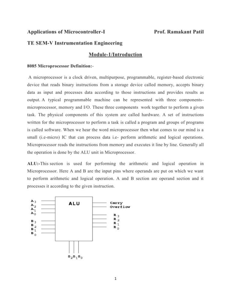
Applications of Microcontroller-I Prof. Ramakant Patil TE SEM-V Instrumentation Engineering Module-1/Introduction 8085 Microprocessor Definition:A microprocessor is a clock driven, multipurpose, programmable, register-based electronic device that reads binary instructions from a storage device called memory, accepts binary data as input and processes data according to those instructions and provides results as output. A typical programmable machine can be represented with three componentsmicroprocessor, memory and I/O. These three components work together to perform a given task. The physical components of this system are called hardware. A set of instructions written for the microprocessor to perform a task is called a program and groups of programs is called software. When we hear the word microprocessor then what comes to our mind is a small (i.e-micro) IC that can process data i.e- perform arithmetic and logical operations. Microprocessor reads the instructions from memory and executes it line by line. Generally all the operation is done by the ALU unit in Microprocessor. ALU:-This section is used for performing the arithmetic and logical operation in Microprocessor. Here A and B are the input pins where operands are put on which we want to perform arithmetic and logical operation. A and B section are operand section and it processes it according to the given instruction. 1 Arithmetic operation:- Like addition, subtraction, multiplication, division etc. Logical Operation:- Like AND,OR,NOT,EX-OR etc all logical operation. Opcode:- A Binary code that indicates the operation to be performed is called as an opcode. Operands:- The data on which the operation is to be performed is known as operand. Instruction:- The combination of opcode and an operand, that can be used to instruct a system is called as an instruction. Instruction set:- A list of all the instructions that can be issued to a system is called as instruction set. Program/Subroutine/Routine:- A set of instructions written in a particular sequence, so as to implement a given task. A subroutine in assembly refers to function as in C/C++. Bus:- A group of lines, pins or signal s having commons functions is termed as the bus. There are three buses in 8085 Microprocessor: 1. Data bus- Microprocessor has 8 bit data bus. It carries data(to receive and to transmit) from memory or to memory. 2. Address bus-Microprocessor has 16 bit address bus. Generally it is used to select the memory or I/O location through which we want to communicate the microprocessor. 3. System bus-It provides control and timing signal to perform the various operation. Memory:-Generally a memory is used for storage purpose. We can store the data, instruction sets etc. Instruction sets are stored in memory in form of binary number. It provides that information to Microprocessor whenever necessary. Microprocessor reads instructions from memory and performs the operation in its ALU section. Results are transferred to Output Section (LCD display, LED, others). It may also store in memory as it needs. There are two types of memory: RAM (Random Access Memory) - It is a type of memory provides the reading and writing both facility. ROM (Read Only Memory) - Data or program stored in ROM can only be read. It cannot be altered. It doesn't provide the writing facility. 8051 Microcontroller Definition:8051 is an 8-bit family of microcontroller developed by Intel in the year 1981. This is one of the most popular families of microcontroller being used all across the world. This microcontroller was also referred as “system on a chip” because it has 128 bytes of RAM, 4Kbytes of ROM, 2 Timers, 1 Serial port, and four ports on a single chip. The CPU can work for only 8bits of data at a time because 8051 is an 8-bit processor. In case the data is larger than 8 bits then it has to be broken into parts so that the CPU can process conveniently. Most manufacturers have put 4Kbytes of ROM even though the quantity of ROM can be exceeded up to 64 K bytes. 2 Operation of Arithmetic and logic Unit (ALU):- A simplified ALU is illustrated in Fig., which uses an arrangement of both combinational and sequential circuit. Their purpose is to perform the basic (though still complex) binary arithmetic. Data passing through the ALU circuit does so on a system of buses, shown by the broad arrows in Fig. These buses consist of groups of wires (usually as 8 parallel bits in simple systems) each carrying a single byte of binary data. In this system, data word A is the primary data source, and data word B is the secondary data source that may be added to, or subtracted from word A. The ALU can also perform other operations. It can increment, add 1 to word A, or decrement, and subtract 1 from it. By complementing (inverting) the logic value of individual bits of the 3 data word A and adding 1 to the result, it is possible to use twos complement arithmetic to perform subtractions. The shift register at the ALU output can also perform a ‘logical shift-left’ on word A by shifting the 8 bits consecutively into the carry bit, alternatively the shift register can create a rotating pattern of bits, rotating left, and using the carry bit as a ninth bit in the sequence, or rotate the 8 bits right ignoring the carry bit. Any of these functions can be selected by the control block, using various combinations of the eight control lines shown in Fig. Putting the correct pattern of 1s and 0s (the control word) on the control lines will cause the ALU to perform the required arithmetic or logical operation on the data being input at A and B. With a control word of 8-bits, this could potentially allow up to 256 different combinations, or control words, which would be more than ample, even for very complex microprocessors or micro controllers. However this basic ALU needs only eight control words to control the different operations available. Evolution of Microprocessor:- 4 Microprocessor Based System:A microprocessor-based system consists primarily of three components-the microprocessor unit (MPU), memory and I/O (input / output). The MPU is the central player; it communicates with memory and I/O devices. Processes data, and controls timing of all its operations. In the microprocessor based computer system, three buses exist for transfer of address, data and control information between the microprocessor and its memory and I/O system. 5 The Microprocessor Unit (MPU) is a programmable logic device with a designed set of instructions. It reads or fetches each instruction, one at a time, from memory and performs data manipulation specified by the instruction; it also reads data from input devices and writes (or sends) data to output devices. When the MPU is executing a program, it communicates frequently with memory and I/0 devices; the process consists of fetch, decode, and execute operations. In addition to processing data according to the instructions written in memory, the MPU needs to respond to various situations described above. External devices should be able to interrupt and request the attention of the MPU. This communication process and related operations between the MPU and the external devices (memory, I/Os) can be classified into two main categories: · Program-initiated operations · Peripheral (or externally) initiated operations. To perform these operations, the MPU requires a group of logic circuits, a set of signals to transfer information, control signals for timing, and clock circuitry; these constitute the architecture. Early microprocessors did not have the necessary circuitry on one chip; the complete units were made up of more than one chip. Therefore, we define here the term Microprocessor Unit (MPU) as a group of device that can perform operations similar to those of the Central Processing Unit (CPU). To communicate with memory and I/Os, the MPU performs four operations: 1. Memory Read: Reads instructions or data from memory. 2. Memory Write: Writes instructions or data into memory. 3. I/O Read: Accepts data from input devices. 6 4. I/O Write: Sends data to output devices. The steps in performing these MPU operations can be summarized as follows (not necessarily in the order listed in every operation): 1. Identify the memory location or the peripheral with its address. 2. Provide timing or synchronization signal. 3. Transfer binary data. Therefore, the MPU requires three sets of communication lines called buses: the first group of lines, called the address bus, to identify the memory location; the second group, called the data bus, to transfer data; and the third group, called the control lines, for timing signals. ADDRESS BUS The addressing is simply a numbering scheme to identify memory registers. For example, a twodigit decimal numbering scheme can identify only 100 items, from 00 to 99. On the other hand, a four-digit numbering scheme can identify 10,000 items, from 0000 to 9999. Thus, the number of bits (address lines) used for addressing by the MPU clearly determines the number of memory registers it can identify. The address lines are generally identified as A0 to Am where m indicates the most significant address bit. Typically, microprocessors such as the 8085, the Z80, and the 6800 have 16 address lines which are capable of addressing as 64K memory. However, recent microprocessors such as the 8086 have 20 address lines, and the 68000 has 23 address lines. DATA BUS These lines are used to transfer data and are bidirectional-data can flow either direction. These lines are identified as D0 to Dn where n signifies the most significant bit (MSB) of the data bus. Again, the size of the data bus determines how large a binary number can be transferred and processed at a time and thus influences the microprocessor architecture considerably. The 8085, the Z80, and the 6800 have eight data lines and thus are called 8-bit microprocessors .On the other hand, the 8086, the 80286 and the 68000 have 16 data lines and are called 16-bit microprocessors. CONTROL SIGNALS (MPU INITIATED) These are individual signal lines generated by the MPU to indicate its operations. The MPU generates a specific signal for each of its four operations-Memory Read. Memory Write, 1/0 Read, and I/O Write. These are timing signals that are used to enable, or activate, peripherals. For example, to fetch (or read) an instruction from a memory location, the MPU sends a timing pulse called Memory Read to enable the memory chip. 7 INPUT AND OUTPUT (I/0) DEVICES These devices are the means through which the MPU communicates with "the outside world." The MPU accepts binary data as input from devices such as keyboards and analog-to-digital (A/D) converters and sends data to output devices such as LEDs or printers. There are two different methods b which an MPU can identify I/O devices : one uses an 8-bit address and the other a 16- bit address. MEMORY It can be classified into two groups: RAM and ROM. RAM is the memory the microcomputer uses in executing and storing programs. This memory should be able to respond fast enough to keep up with the execution speed of the microprocessor. Therefore, it should be random-access memory, meaning that the microprocessor should be able to access information from any register with the same speed. Storage memory includes examples such as magnetic disks and tapes. This memory is used to store programs and results after the completion of program execution. Information stored in' these memories is nonvolatile, meaning information remains intact even if the system is turned off. Generally, these memory devices are not a part of any system; they are made part of the system only when stored programs need to be accessed. The microprocessor cannot execute or directly process programs stored in these devices: programs must be copied into the prime memory first. CISC Architecture:The CISC approach attempts to minimize the number of instructions per program, sacrificing the number of cycles per instruction. Computers based on the CISC architecture are designed to decrease the memory cost. Because, the large programs need more storage, thus increasing the memory cost and large memory becomes more expensive. To solve these problems, the number of instructions per program can be reduced by embedding the number of operations in a single instruction, thereby making the instructions more complex. 8 MUL loads two values from the memory into separate registers in CISC. CISC uses minimum possible instructions by implementing hardware and executes operations. Instruction Set Architecture is a medium to permit communication between the programmer and the hardware. Data execution part, copying of data, deleting or editing is the user commands used in the microprocessor and with this microprocessor the Instruction set architecture is operated. The main keywords used in the above Instruction Set Architecture are as below Instruction Set: Group of instructions given to execute the program and they direct the computer by manipulating the data. Instructions are in the form – Opcode (operational code) and Operand. Where, opcode is the instruction applied to load and store data, etc. The operand is a memory register where instruction applied. Addressing Modes: Addressing modes are the manner in the data is accessed. Depending upon the type of instruction applied, addressing modes are of various types such as direct mode where 9 straight data is accessed or indirect mode where the location of the data is accessed. Processors having identical ISA may be very different in organization. Processors with identical ISA and nearly identical organization is still not nearly identical. CPU performance is given by the fundamental law Thus, CPU performance is dependent upon Instruction Count, CPI (Cycles per instruction) and Clock cycle time. And all three are affected by the instruction set architecture. Instruction Count of the CPU This underlines the importance of the instruction set architecture. There are two prevalent instruction set architectures Examples of CISC PROCESSORS IBM 370/168 – It was introduced in the year 1970. CISC design is a 32 bit processor and four 64-bit floating point registers. VAX 11/780 – CISC design is a 32-bit processor and it supports many numbers of addressing modes and machine instructions which is from Digital Equipment Corporation. Intel 80486 – It was launched in the year 1989 and it is a CISC processor, which has instructions varying lengths from 1 to 11 and it will have 235 instructions. CHARACTERISTICS OF CISC ARCHITECTURE Instruction-decoding logic will be Complex. One instruction is required to support multiple addressing modes. 10 Less chip space is enough for general purpose registers for the instructions that are 0operated directly on memory. Various CISC designs are set up two special registers for the stack pointer, handling interrupts, etc. MUL is referred to as a “complex instruction” and requires the programmer for storing functions. RISC Architecture:RISC (Reduced Instruction Set Computer) is used in portable devices due to its power efficiency. For Example, Apple iPod and Nintendo DS. RISC is a type of microprocessor architecture that uses highly-optimized set of instructions. RISC does the opposite, reducing the cycles per instruction at the cost of the number of instructions per program Pipelining is one of the unique feature of RISC. It is performed by overlapping the execution of several instructions in a pipeline fashion. It has a high performance advantage over CISC. RISC processors take simple instructions and are executed within a clock cycle 11 RISC ARCHITECTURE CHARACTERISTICS Simple Instructions are used in RISC architecture. RISC helps and supports few simple data types and synthesize complex data types. RISC utilizes simple addressing modes and fixed length instructions for pipelining. RISC permits any register to use in any context. One Cycle Execution Time The amount of work that a computer can perform is reduced by separating “LOAD” and “STORE” instructions. RISC contains Large Number of Registers in order to prevent various number of interactions with memory. In RISC, Pipelining is easy as the execution of all instructions will be done in a uniform interval of time i.e. one click. In RISC, more RAM is required to store assembly level instructions. Reduced instructions need a less number of transistors in RISC. RISC uses Harvard memory model means it is Harvard Architecture. A compiler is used to perform the conversion operation means to convert a high-level language statement into the code of its form. RISC & CISC Comparison:- MUL instruction is divided into three instructions “LOAD” – moves data from the memory bank to a register “PROD” – finds product of two operands located within the registers 12 “STORE” – moves data from a register to the memory banks The main difference between RISC and CISC is the number of instructions and its complexity. RISC Vs CISC CISC and RISC designs are the two options. CISC designs involve very complex architectures, including a large number of instructions and addressing modes, whereas RISC designs involve simplified instruction set and adapt it to the real requirements of user programs. Multiplication of two Numbers in Memory: If the main memory is divided into areas that are numbered from row1:column 1 to row 5 :column 4. The data is loaded into one of four registers (A, B, C, or D). To find multiplication of two numbers- One stored in location 1:3 and other stored in location 4:2 and store back result in 1:3. 13 Multiplication of Two Numbers The Advantages of RISC architecture: RISC architecture has a set of instructions, so high-level language compilers can produce more efficient code It allows freedom of using the space on microprocessors because of its simplicity. Many RISC processors use the registers for passing arguments and holding the local variables. RISC functions use only a few parameters, and the RISC processors cannot use the call instructions, and therefore, use a fixed length instruction which is easy to pipeline. The speed of the operation can be maximized and the execution time can be minimized. Very less number of instructional formats, a few numbers of instructions and a few addressing modes are needed. The Disadvantages of RISC architecture: Mostly, the performance of the RISC processors depends on the programmer or compiler as the knowledge of the compiler plays a vital role while changing the CISC code to a RISC code While rearranging the CISC code to a RISC code, termed as a code expansion, will increase the size. And, the quality of this code expansion will again depend on the compiler, and also on the machine’s instruction set. 14 The first level cache of the RISC processors is also a disadvantage of the RISC, in which these processors have large memory caches on the chip itself. For feeding the instructions, they require very fast memory systems. Advantages of CISC architecture: Microprogramming is easy assembly language to implement, and less expensive than hard wiring a control unit. The ease of micro coding new instructions allowed designers to make CISC machines upwardly compatible: As each instruction became more accomplished, fewer instructions could be used to implement a given task. Disadvantages of CISC architecture: The performance of the machine slows down due to the amount of clock time taken by different instructions will be dissimilar Only 20% of the existing instructions is used in a typical programming event, even though there are various specialized instructions in reality which are not even used frequently. The conditional codes are set by the CISC instructions as a side effect of each instruction which takes time for this setting – and, as the subsequent instruction changes the condition code bits – so, the compiler has to examine the condition code bits before this happens. Model Questions Q.1 Compare between RISC and CISC processor. [Dec. 2014, 4Marks] Q.2 Draw and explain any one microprocessor based system. [Dec. 2014, 5Marks] Q.3 List the important features of RISC and CISC processor. [May 2015, 4Marks] Q.4 Explain the evaluation of microprocessor. [May 2015, 5Marks] 15
