Experiment#7
advertisement
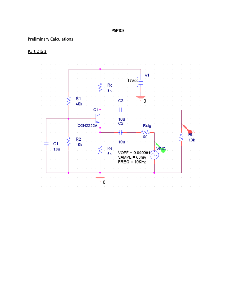
PSPICE Preliminary Calculations Part 2 & 3 2.0V 1.0V 0.0V -1.0V -2.0V -3.0V 4.00ms 4.05ms V(VSIG:+) V(C3:1) 4.10ms 4.15ms 4.20ms 4.25ms Time Part 2 RC = 8KΩ VCE (Experimental) = 10.64V VCE (Calculated - PSPICE) = 10.6V IC (Experimental) = 0.475 mA IC (Calculate - PSPICE) = 0.456 mA Part 3 Vin = 60 mV Vout = 4.24V AV (Experimental) = 70.6 V/V AV (Calculated) = 70.6 V/V 4.30ms 4.35ms 4.40ms 4.45ms 4.50ms Comparing our experimental values with our PSPICE values, we found our calculated resistances to be very accurate. This means that our circuit values were calculated and implemented almost perfectly, with an error of less than 10%. You can see that our experimental output waveform, Figure (INSERT FIGURE HERE) is very similar, if not identical to our PSPICE output waveform, Figure (INSERT FIGURE HERE). Our measured Av (output gain) matches our PSPICE output gain perfectly. Part 4 2.0V 1.0V -0.0V -1.0V -2.0V -3.0V -4.0V 4.00ms 4.05ms V(VSIG:+) V(C3:1) 4.10ms 4.15ms 4.20ms 4.25ms 4.30ms 4.35ms 4.40ms 4.45ms 4.50ms Time Part 4 When distortion begins (output swing > 3V): Vin = 100mV Vout (Calculated) = 5.84V Vout (Experimental) = 5.76V We used PSPICE to measure the output voltage at which our Vout begins to show distortion, meaning the maximum voltage our amplifier is able to drive the output. In both our experimental and PSPICE circuits, we were able to drive the load resistor to around 5.8V. This surpasses the specified output swing of at least 3V. Part 5 2.0V 1.0V 0V -1.0V -2.0V 4.00ms 4.05ms V(VSIG:+) V(C3:1) 4.10ms 4.15ms 4.20ms 4.25ms 4.30ms 4.35ms 4.40ms 4.45ms 4.50ms Time Part 5 V1 (Vout) (Calculated) = 4.24 V V1 (Vout) (Experimental) = 4.24 V Total Resistance Inserted: 130Ω V2 (Vout) (Calculated) = 2.17V V2 (Vout) (Experimental) = 2.24V Zi = 86.3Ω In experiment 6, we learned that we could essentially guess and check with various input resistors to find out what the input impedance of our circuit was. This was done by inserting an additional input resistor (Rn) with a value such that our Vn will be half the input voltage (Vin) of the original circuit. We know this because whenever a voltage is passed through 2 equivalent resistors in series, the voltage is divided in half. In Figure (INSERT FIGURE HERE), we see that our original PSPICE input voltage is 4.24V, and when a 130Ω resistor is inserted, the voltage across that resistor becomes 2.24V. Therefore we can conclude that our input impedance (Zin) is approximately 130Ω. This coincides with the generalization that common base amplifiers have low input impedance, which explains why they are commonly used as the 2 nd stage in multistage amplifiers. Part 6 1.0V -0.0V -1.0V -2.0V 4.00ms 4.05ms V(VSIG:+) V(C3:1) 4.10ms 4.15ms 4.20ms 4.25ms 4.30ms 4.35ms 4.40ms 4.45ms 4.50ms Time Part 6 Removing RL: V1 (Vout) = 4.24V Total Resistance Inserted: 3kΩ V2 (Vout) (Calculated) = 2.09V V2 (Vout) (Experimental) = 2.40V Zi (Experimental) = 7.67KΩ (Should be approximately the same as RC) Note: PSPICE did not work properly with respect to finding V2, therefore, the experimental V2 was used to calculate the Zi. As with finding input impedance, we use a similar guess and check method to find output impedance. This is done by first measuring the output voltage with an open (infinite) load resistance. Next, we increase the original load resistance such that the output voltage (open load) is divided in half. Above in Figure (INSERT FIGURE HERE), we can see that inserting a 3kΩ resistor changes our output voltage from 4.24V to 2.4V. Therefore our output impedance (Zout) is approximately 3kΩ.
