Supplementary material for publication
advertisement
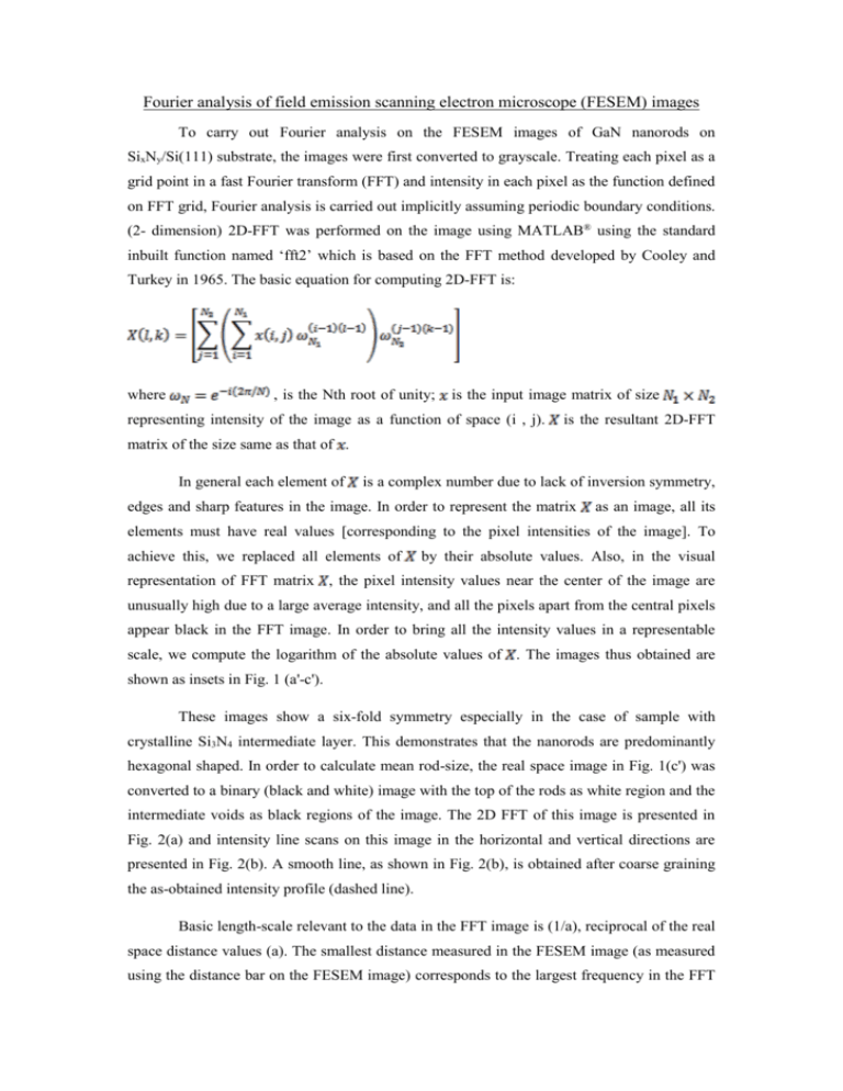
Fourier analysis of field emission scanning electron microscope (FESEM) images To carry out Fourier analysis on the FESEM images of GaN nanorods on SixNy/Si(111) substrate, the images were first converted to grayscale. Treating each pixel as a grid point in a fast Fourier transform (FFT) and intensity in each pixel as the function defined on FFT grid, Fourier analysis is carried out implicitly assuming periodic boundary conditions. (2- dimension) 2D-FFT was performed on the image using MATLAB® using the standard inbuilt function named ‘fft2’ which is based on the FFT method developed by Cooley and Turkey in 1965. The basic equation for computing 2D-FFT is: where , is the Nth root of unity; is the input image matrix of size representing intensity of the image as a function of space (i , j). is the resultant 2D-FFT matrix of the size same as that of . In general each element of is a complex number due to lack of inversion symmetry, edges and sharp features in the image. In order to represent the matrix as an image, all its elements must have real values [corresponding to the pixel intensities of the image]. To achieve this, we replaced all elements of by their absolute values. Also, in the visual representation of FFT matrix , the pixel intensity values near the center of the image are unusually high due to a large average intensity, and all the pixels apart from the central pixels appear black in the FFT image. In order to bring all the intensity values in a representable scale, we compute the logarithm of the absolute values of . The images thus obtained are shown as insets in Fig. 1 (a'-c'). These images show a six-fold symmetry especially in the case of sample with crystalline Si3N4 intermediate layer. This demonstrates that the nanorods are predominantly hexagonal shaped. In order to calculate mean rod-size, the real space image in Fig. 1(c') was converted to a binary (black and white) image with the top of the rods as white region and the intermediate voids as black regions of the image. The 2D FFT of this image is presented in Fig. 2(a) and intensity line scans on this image in the horizontal and vertical directions are presented in Fig. 2(b). A smooth line, as shown in Fig. 2(b), is obtained after coarse graining the as-obtained intensity profile (dashed line). Basic length-scale relevant to the data in the FFT image is (1/a), reciprocal of the real space distance values (a). The smallest distance measured in the FESEM image (as measured using the distance bar on the FESEM image) corresponds to the largest frequency in the FFT image. This was used to calibrate the inverse length scales in the FFT image. The intensity peaks in the FFT image correspond to the length scales that are most dominant in the real space FESEM images. These correspond to the dH and dv values indicated in Fig. 2(b). Thus, 1/dH and 1/dV values correspond to the average length scales (nearest rod-rod distance) in the horizontal and vertical directions respectively in Fig. 1 (c'). In order to extract the mean rod size from the dH and dV values, the average ratios of the length of the region occupied by rods to that occupied by the voids along horizontal and vertical directions were calculated from the real space image data (x) and found to be 2.04 and 2.08 respectively. Using these values along with mean rod-rod distances as calculated above, we find the mean rod size to be 163 nm, which was in good agreement with the size calculated using line scans (160 nm). One can also obtain the information regarding the arrangement of nanorods relative to each other by analyzing the FFT images. This long length-scale information corresponds to short frequency scale information (near to the center of the FFT image). Thus, upon adjusting the contrast of the image we analyze the pixels in the Fourier image close to the center of the image (zero frequency). We observe a 30° (± 8°) rotational mismatch between the six-fold symmetry axes corresponding to the hexagonal shape of the rods and the hexagonal in-plane ordering of the nanorods. This is schematically shown in Fig. 2(e).

![Y = fft(X,[],dim)](http://s2.studylib.net/store/data/005622160_1-94f855ed1d4c2b37a06b2fec2180cc58-300x300.png)
