NTHU ESS5810 Advance Micro System Fabrication and Lab F. G.
advertisement
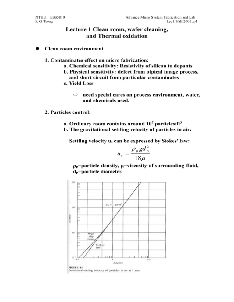
NTHU ESS5810 F. G. Tseng Advance Micro System Fabrication and Lab Lec1, Fall/2001, p1 Lecture 1 Clean room, wafer cleaning, and Thermal oxidation Clean room environment 1. Contaminates effect on micro fabrication: a. Chemical sensitivity: Resistivity of silicon to dopants b. Physical sensitivity: defect from otpical image process, and short circuit from particular contaminates c. Yield Loss need special cares on process environment, water, and chemicals used. 2. Particles control: a. Ordinary room contains around 107 particles/ft3 b. The gravitational settling velocity of particles in air: Settling velocity us can be expressed by Stokes’ law: p gd p2 us 18 p=particle density, =viscosity of surrounding fluid, dp=particle diameter. NTHU ESS5810 F. G. Tseng Advance Micro System Fabrication and Lab Lec1, Fall/2001, p2 c. Particles smaller than 0.05 m is not significant in fabrication process. Because of the low settling speed in minuscule, they form airbone flying in the air and not easily to be deposited on wafers. Particle size above 0.5 m is very important. 3. Clean room a. Class x clean room has fewer than X particles/ft3 of size above 0.5 m. b. Schematic of a clean room: (using filtration methods and laminar flow to filter out particles) c. The goal of laminar flow: prevent turbulence mixing, particles cross the boundary through convective and diffusive fluxes. NTHU ESS5810 F. G. Tseng Advance Micro System Fabrication and Lab Lec1, Fall/2001, p3 d. Tow mechanisms for filtration: block particle larger than the pore of filter, stick particles for smaller sizes (for HEPA (Hight efficiency Particular air) filter pore size of 5 m fiber radius, some circumstance can have most popular particle size in 0.13 m) e. Pressure drop, Darcy’s law: P kU 0 Z =air viscosity, Z=thickness of the filter medium, U0=superficial velocity (approach velocity to the filter.) Wafer cleaning process The goal of wafer cleaning: to remove contamination from wafer before next process. 1. Contamination classification NTHU ESS5810 F. G. Tseng Advance Micro System Fabrication and Lab Lec1, Fall/2001, p4 Particulates: (1) Particulate matter (airborne bacteria, dust, abrasive particles: SiC, Al2O3, diamond power, lint from filter, human skin or clothing), (2) Traces of organic (photoresist, Grease, Wax from cutting oil or physical handling, finger print, plasticizers from containers and wrapping materials) (3) Light metal ion (Na, K... from etchant impurities) (4) Heavy metal impurities (Ca, Co, Hg, Cu, Au, Fe, Ag, Ni…electrodeposition from etchant) Films: (2) Solvent residues (leave stain, causing poor resist adhesion and increasing undercutting during etching), fully rinsing and apply next rinsing step before drying out of the previous rinsing solvent is necessary (3) Photoresist developer residues (overconcentration of dissolved photoresist, positive PR: react with carbon dioxide in air, negative PR: solvent evaporated), fully rinse and 2 step developing can help. (4) oil films (from not filtered nitrogen, air or other gas lines) (5) silicone films (causing resist wetting and adhesion problems, coming from hand cream, lubricants, cutting oils, human skin oils, detergents, usually give the wafer a hydrophobic surface resisting aqueous cleaning), using atomizing a layer of water on the surface to check the uniformity. (6) Metallic films ( from the ion in etchants and resist stripper, those ions may replace silicon or entrapped on wafers): good three steps rinse and a spry rinse can reduce the later, but not the former. (7) Water stains NTHU ESS5810 F. G. Tseng Advance Micro System Fabrication and Lab Lec1, Fall/2001, p5 (caused by the impurity of water, posing resist adhesion problem) (8) Native oxide (~ 50 Å) Using dilute HF to remove. 2. DI Water (deionized water, 18 Mohm-cm at 25∘C, <0.25 μm particles, <1.2 colonies of bacteria/mL) is desired throughout the fabrication process to reduce ion contimation. 3. Silicon wafer cleaning methods: Silicon wafer Standard cleaning: For organic removal by Solvent, necessary before any process steps: 1. Immerse in acetone for 3 min 2. Immerse in methyl alcohol (or IPA, iso-proponal alcohol) for 3 min 3. Wash in DI water for 3 min 4. Nitrogen blow dry Silicon wafer Piranha cleaning: For remove light-metal-ion contamination and Residual Organic( not good if the wafer already has metal structures): 1. Immerse in a (6:1:1) solution of H2O-HCl-H2O2 (can be replaced by (Piranha bath: H2O2: H2SO4 =1:10) for 10 min at temp of 75-80∘C 2. Quench the solution under running DI water for 1 min. 3. Wash in DI water for 20 min Note: to Remove hard baked PR without damage the metal structures already on the wafer, using organic stripper (for example, AZ 300T at 80C for AZ resist removal) Silicon wafer Pre-furnace cleaning (RCA cleaning): A. Organic removal by Solvent: NTHU ESS5810 F. G. Tseng Advance Micro System Fabrication and Lab Lec1, Fall/2001, p6 1. Immerse in boiling trichloroethylene (TCE) for 3 min (not use in school) 2. Immerse in boiling acetone for 3 min (room temp in the lab) 3. Immerse in boiling methyl alcohol for 3 min (room temp in the lab) 4. Wash in DI water for 3 min B. Removal of Residual Organic/Heavy metal impurities 1. Immerse in a (5:1:1) solution of H2O-HH4OH-H2O2 at 75-80∘C for 10 min. (RCA I) 2. Quench the solution under running DI water for 1 min. 3. Wash in DI water for 5 min C. Hydrous Oxide removal: 1. Immerse in a (1:50) solution of HF-H2O for 40-60 sec 2. Wash in running DI water with agitation for 30 sec. D. Light-metal-ion contamination removal: 1. Immerse in a (6:1:1) solution of H2O-HCl-H2O2 (can be replaced by (Piranha bath: H2O2: H2SO4 =1:10) for 10 min at temp of 75-80∘C 2. Quench the solution under running DI water for 1 min. 3. Wash in DI water for 20 min Note: chloride ions is easier to be removed for weak van der waals forces than fluoride ions. Silicon wafer dry cleaning: a. To avoid residue left behind wet chemical etching, and chemical disposal problem b. High temp burn off: in oxidation tube at 900-1200C c. Low temp ashing: Oxygen plasma—descum after development. (however, dry oxygen plasma may also deposit polymer type residue onto wafers surface, depending on the chamber cleanness.) NTHU ESS5810 F. G. Tseng Advance Micro System Fabrication and Lab Lec1, Fall/2001, p7 d. Dry etching plasma: CF4:O2 e. To cleanly remove negative resist: 650C heat treatment (ash) in air. f. Resist film wet stripper: Piranha (H2SO4:H2O2=10:1), or HNH4:H2O2:H2O=1:1:5. NTHU ESS5810 F. G. Tseng Advance Micro System Fabrication and Lab Lec1, Fall/2001, p8 Thermal oxidation 1. SiO2 melting point: 1732 C, growth 1 µm SiO2 Consume 0.44 µm Silicon. It is a high quality insulator and good barrier material during impurity diffusion. 2. Diffusivity: D D0 e E A / kT D0=Diffusion constant, EA=activation energy of the diffusion species in eV/Molecule. K=Boltzmann’s constant, 8.62e-5 eV/K, T= temperature. NTHU ESS5810 F. G. Tseng Advance Micro System Fabrication and Lab Lec1, Fall/2001, p9 3. Oxide formation: Dry Oxide: Si+O2 SiO2 Wet Oxide: Si+2H2O SiO2+2H2 Note: 1. wet thermal oxide is faster in long time oxide growth, but slower in short times (<160 A), because H2O’s diffusion rate is slower than O2. However, water can form hydroxyl groups within the Si-O-Si network, which opens the solid structure and permits much more rapid diffusion of the oxidants H2O and O2 the reactive interface. 2.Wet thermal oxide is more porous than dry oxide, so is not as good as dry oxide for gate oxide. 4. Kinetics of Oxide Growth: Silicon Silicon Dioxide N0 J N1 Diffusion process: J D N D( N 0 N1 ) x x (2-1) where x is thickness of the oxide at a given time. This is Henry’s law. NTHU ESS5810 F. G. Tseng p10 Advance Micro System Fabrication and Lab Lec1, Fall/2001, Reaction process: J kN1 (2-2) Where k is the interfacial reaction rate constant. Combining Eqs. (2-1) and (2-2) gives: J DN 0 x D/k (2-3) The rate of change of the oxide layer thickness is given by: dx J DN 0 / n dt n x D / k (2-4) Were n is the number of molecules of the oxidizing impurity that are incorporated into unit volume of the oxide. Solving this equation to the boundary condition that x=0 at t=0, gives x2 2DN 0 2D x t k n (2-5) So that x 2N 0 k 2t 1/ 2 D [(1 ) 1] k Dn (2-6) Define A=2D/k, B=2DN0/n, when t is small (<<1, thickness <500), equation (2-6) can be reduced to: x B t A (reaction limit) (2-7) (diffusion limit) (2-8) and for large t: x Bt NTHU ESS5810 F. G. Tseng p11 5. Thickness vs. Time and Temp: 7. Selective Oxidation: Advance Micro System Fabrication and Lab Lec1, Fall/2001, NTHU ESS5810 F. G. Tseng p12 Advance Micro System Fabrication and Lab Lec1, Fall/2001, 8. Color: Reference: 1. Introduction to Microelectronic Fabrication, Richard C. Jaeger, Addison-Wesley Publishing Company, Inc, 1998. 2. Integrated circuit fabrication technology, David J. Elliott, second edition, McGRAW-HILL, 1989. 3. Process engineering analysis in semiconductor device fabrication, Stanley NTHU ESS5810 F. G. Tseng p13 Advance Micro System Fabrication and Lab Lec1, Fall/2001, Middleman, and Arthur K. Hochberg, McGRAW-HILL, international editions, 1993.
