MOS Transistor Definitions - Electrical & Computer Engineering
advertisement
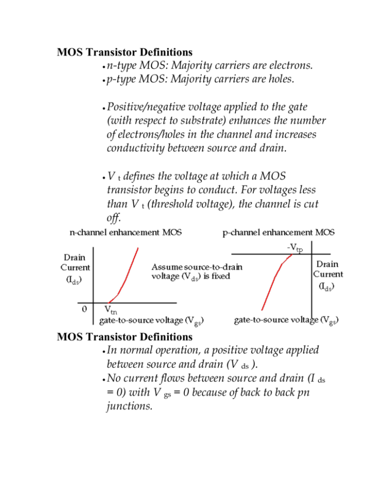
MOS Transistor Definitions n-type MOS: Majority carriers are electrons. p-type MOS: Majority carriers are holes. Positive/negative voltage applied to the gate (with respect to substrate) enhances the number of electrons/holes in the channel and increases conductivity between source and drain. V t defines the voltage at which a MOS transistor begins to conduct. For voltages less than V t (threshold voltage), the channel is cut off. MOS Transistor Definitions In normal operation, a positive voltage applied between source and drain (V ds ). No current flows between source and drain (I ds = 0) with V gs = 0 because of back to back pn junctions. For n-MOS, with V gs > V tn , electric field attracts electrons creating channel. Channel is p-type silicon which is inverted to ntype by the electrons attracted by the electric field. n-MOS Enhancement Transistor Physics Three modes based on the magnitude of V gs : accumulation, depletion and inversion. n-MOS Enhancement Transistor Physics n-MOS Enhancement Transistor With V ds non-zero, the channel becomes smaller closer to the drain. When V ds <= V gs - V t (e.g. V ds = 3V, V gs = 5V and V t = 1V), the channel reaches the drain (since V gd > V t ). This is termed linear , resistive or nonsaturated region. I ds is a function of both V gs and V ds . n-MOS Enhancement Transistor When V ds > V gs - V t (e.g. V ds = 5V, V gs = 5V and V t = 1V), the channel is pinched off close to the drain (since V gd < V t ). This is termed saturated region. I ds is a function of V gs , almost independent of V ds . MOS Enhancement Transistor MOS transistors can be modeled as a voltage controlled switch. I ds is an important parameter that determines the behavior, e.g., the speed of the switch. What are the parameters that effect the magnitude of I ds ? (Assume V gs and V ds are fixed, e.g. 5V). The distance between source and drain (channel length). The channel width. The threshold voltage. The thickness of the gate oxide layer. The dielectric constant of the gate insulator. The carrier (electron or hole) mobility. Summary of normal conduction characteristics: Cut-off : accumulation, I ds is essentially zero. Nonsaturated : weak inversion, I ds dependent on both V gs and V ds . Saturated : strong inversion, I ds is ideally independent of V ds . Threshold Voltage V t is also an important parameter. What effects its value? Most are related to the material properties. In other words, V t is largely determined at the time of fabrication, rather than by circuit conditions, like I ds . For example, material parameters that effect V t include: The gate conductor material (poly vs. metal). The gate insulation material (SiO 2 ). The thickness of the gate material. The channel doping concentration. However, V t is also dependent on V sb (the voltage between source and substrate), which is normally 0 in digital devices. Temperature: changes by -2mV/degree C for low substrate doping levels. Threshold Voltage The expression for threshold voltage is given as: Threshold Voltage Threshold voltage (cont.): Typical values of V t for n and p-channel transistors are +/- 700mV. Threshold Voltage From equations, threshold voltage may be varied by changing: The doping concentration (N A ). The oxide capacitance (C ox ). Surface state charge (Q fc ). As you can see, it is often necessary to adjust V t . Two methods are common: Change Q fc by introducing a small doped region at the oxide/substrate interface via ion implantation. Change C ox by using a different insulating material for the gate. o A layer of Si 3 N 4 (silicon nitride) with a relative permittivity of 7.5 is combined with a layer of silicon dioxide (relative permittivity of 3.9). o This results in a relative permittivity of about 6. o For the same thickness dielectric layer, C ox is larger using the combined material, which lowers V t . Body Effect In digital circuits, the substrate is usually held at zero. o The sources of n-channel devices, for example, are also held at zero, except in cases of series connections, e.g., The source-to-substrate (V sb ) may increase at this connections, e.g. V sbN1 = 0 but V sbN2 /= 0. V sb adds to the channel-substrate potential: Basic DC Equations Ideal first order equation for cut-off region: Ideal first order equation for linear region: Ideal first order equation for saturation region: with the following definitions: Basic DC Equations Process dependent factors: . Geometry dependent factors: W and L. Voltage-current characteristics of the n- and ptransistors. Beta calculation Transistor beta calculation example: o Typical values for an ntransistor in 1 micron technology: o o Compute beta: How does this beta compare with pdevices: n-transistor gains are approximately 2.8 times larger than p-transistors. Inverter voltage transistor characteristics Inverter DC characteristics Beta Ratios Region C is the most important region. A small change in the input voltage, V in , results in a LARGE change in the output voltage, V out . This behavior describes an amplifier, the input is amplified at the output. The amplification is termed transistor gain, which is given by beta. Both the n and p-channel transistors have a beta. Varying their ratio will change the characteristics of the output curve. Beta Ratios Therefore, the o does NOT affect switching performance. What factor would argue for a ratio of 1 for o Load capacitance ! ? The time required to charge or discharge a capacitive load is equal when . Since beta is dependent W and L, we can adjust the ratio by changing the sizes of the transistor channel widths, by making p-channel transistors wider than n-channel transistors. Noise Margins A parameter that determines the maximum noise voltage on the input of a gate that allows the output to remain stable. Two parameters, Low noise margin (NM L ) and High noise margin (NM H ). NM L = difference in magnitude between the max LOW output voltage of the driving gate and max LOW input voltage recognized by the driven gate. Noise Margins Ideal characteristic: V IH = V IL = (V OH +V OL )/2. This implies that the transfer characteristic should switch abruptly (high gain in the transition region). V IL found by determining unity gain point from V OH . Pseudo-nMOS Inverter Therefore, the shape of the transfer characteristic and the V OL of the inverter is affected by the ratio . In general, the low noise margin is considerably worse than the high noise margin for PseudonMOS. Pseudo-nMOS was popular for high-speed circuits, static ROMs and PLAs. Pseudo-nMOS Example: Calculation of noise margins: The transfer curve for the pseudo-nMOS inverter can be used to calculate the noise margins of identical pseudo-nMOS inverters
