FET
advertisement
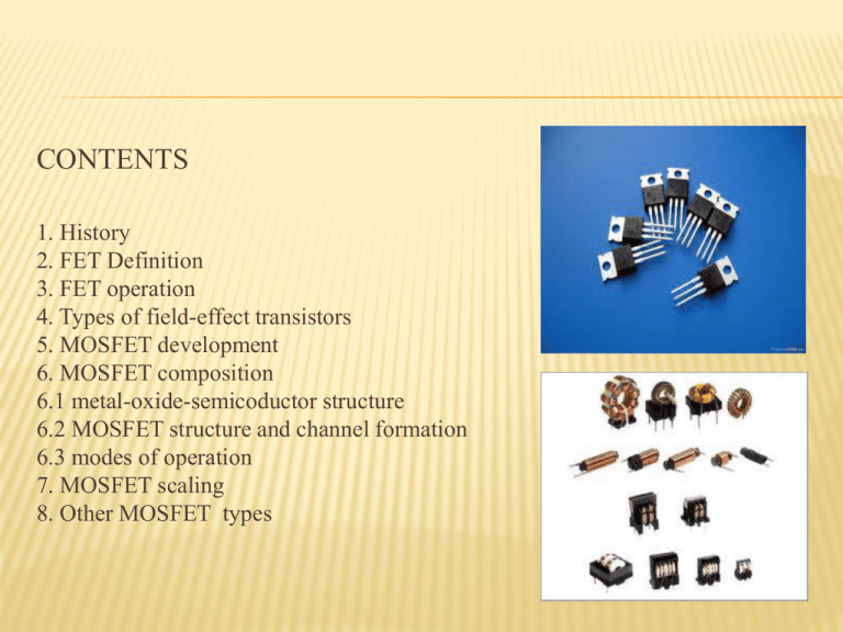
CONTENTS 1. History 2. FET Definition 3. FET operation 4. Types of field-effect transistors 5. MOSFET development 6. MOSFET composition 6.1 metal-oxide-semicoductor structure 6.2 MOSFET structure and channel formation 6.3 modes of operation 7. MOSFET scaling 8. Other MOSFET types History The principle of field-effect transistors was first patented by Julius Edgar Lilienfeld in 1925 and by Oskar Heil in 1934, but practical semi-conducting devices were only developed much later after the transistor effect was observed and explained by the team of William Shockley at Bell Labs in 1947. Definition of a FET The field-effect transistor (FET) is a generic term for a device that controls current through a circuit via an applied voltage, i.e. it behaves like a voltagecontrolled resistor. A FET has three terminals: gate: as in the “gate” keeper of the current source: the source of the current drain: the destination of the current FETs can be made in NPN or PNP variety. FETs are “Unipolar” (conduct either electrons or holes, not both) FET operation The FET controls the flow of electrons (or electron holes) from the source to drain. The FET operation is as follows: apply a voltage to the gate this voltage sets up an electric field in the “body” of the device electric field inhibits/supports the flow of charge from source to drain Depletion mode device in an n-channel depletion-mode device, a negative gate-to-source voltage causes a depletion region to expand in width and encroach on the channel from the sides, narrowing the channel. If the depletion region expands to completely close the channel, the resistance of the channel from source to drain becomes large, and the FET is effectively turned off like a switch. Enhancement-mode device in an n-channel enhancement-mode device, a positive gate-to-source voltage is necessary to create a conductive channel.The positive voltage attracts free-floating electrons within the body towards the gate, forming a conductive channel. Further gate-to-source voltage increase will attract even more electrons towards the gate which are able to create a conductive channel from source to drain; this process is called inversion. Types of field-effect transistors Field-effect transistors are also distinguished by the method of insulation between channel and gate. Types of FETs are: The DEPFET is a FET formed in a fully-depleted substrate and acts as a sensor. he DNAFET is a specialized FET that acts as a biosensor, by using a gate made of single-strand DNA molecules to detect matching DNA strands. The HEMT (High Electron Mobility Transistor), also called an HFET . The IGBT (Insulated-Gate Bipolar Transistor) is a device for power control. The ISFET is an Ion-Sensitive Field Effect Transistor used to measure ion concentrations in a solution. he JFET (Junction Field-Effect Transistor) uses a reverse biased p-n junction to separate the gate from the body. The MODFET (Modulation-Doped Field Effect Transistor). The MOSFET (Metal–Oxide–Semiconductor Field-Effect Transistor) utilizes an insulator (typically SiO2) between the gate and the body. The DGMOSFET is a MOSFET with dual gates. The NOMFET is a Nanoparticle Organic Memory Field-Effect Transistor. The OFET is an Organic Field-Effect Transistor using an organic semiconductor in its channel. The most commonly used FET is the MOSFET MOSFET development MOSFET composition Usually the semiconductor of choice is silicon, but some chip manufacturers, most notably IBM and Intel, recently started using a chemical compound of silicon and germanium (SiGe) in MOSFET. many semiconductors with better electrical properties than silicon, such as gallium arsenide, do not form good semiconductor-to-insulator interfaces, thus are not suitable for MOSFETs. The gate is separated from the channel by a thin insulating layer, traditionally of silicon dioxide and later of silicon oxynitride. When a voltage is applied between the gate and body terminals, the electric field generated penetrates through the oxide and creates an "inversion layer" or "channel" at the semiconductor-insulator interface. The inversion channel is of the same type, P-type or N-type, as the source and drain, thus it provides a channel through which current can pass. MOSFET structure and channel formation in MOSFET the terminals , (source and drain), each connected to individual highly doped regions that are separated by the body region. These regions can be either p or n type, but they must both be of the same type, and of opposite type to the body region. The source and drain (unlike the body) are highly doped as signified by a '+' sign after the type of doping. N- and P- Channel MOSFET and channel formation If the MOSFET is an n-channel or nMOS FET, then the source and drain are 'n+' regions and the body is a 'p' region. with sufficient gate voltage, holes from the body are driven away from the gate, forming an inversion layer or nchannel at the interface between the p region and the oxide. This conducting channel extends between the source and the drain, and current is conducted through it when a voltage is applied between source and drain. Increasing the voltage on the gate leads to a higher electron density in the inversion layer and therefore increases the current flow between the source and drain. If The P and N regions are reversed from the P-Channel device. Modes of operation There are two basic modes of operation of FET’s —depletion and enhancement. Depletion mode, refers to the decrease of carriers in the channel due to variation in gate voltage. Enhancement mode refers to the increase of carriers in the channel due to application of gate voltage. MOSFET scaling Over the past decades, the MOSFET has continually been scaled down in size; typical MOSFET channel lengths were once several micrometres, but modern integrated circuits are incorporating MOSFETs with channel lengths of tens of nanometers. Intel began production of a process featuring a 32 nm feature size (with the channel being even shorter) in late 2009. Historically, the difficulties with decreasing the size of the MOSFET have been associated with the semiconductor device fabrication process, the need to use very low voltages, and with poorer electrical performance necessitating circuit redesign and innovation (small MOSFETs exhibit higher leakage currents, and lower output resistance,). Other MOSFET types Dual gate MOSFET in dual gate MOSFET both gates control the current in the device. It is commonly used for small signal devices in radio frequency applications where the second gate is normally used for gain control or mixing and frequency conversion. FinFET The Finfet, is a double gate device, one of a number of geometries being introduced to mitigate the effects of short channels and reduce draininduced barrier lowering. Power MOSFET Power MOSFETs have a different structure than the one presented above. the structure is vertical and not planar. it is possible for the transistor to sustain both high blocking voltage and high current.

