Semiconductor Heterostructures and their Application
advertisement
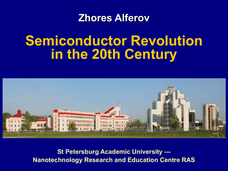
Zhores Alferov Semiconductor Revolution in the 20th Century St Petersburg Academic University — Nanotechnology Research and Education Centre RAS • • • • • • • Introduction Semiconductor research in 1930th Transistor discovery Discovery of laser–maser principle and birth of quantum optoelectronics Invention and development of the silicon chips Heterostructure research “God-made” and “Man-made” crystals Problems and future trends 2 Polytechnical Institute Ioffe seminar at the Polytechnical Institute. 1916 3 Yakov Frenkel 4 One of the last Ioffe photo. September 1960 5 Laboratory demo model of the first bipolar transistor Schematic plot of the first point-contact transistor 6 The Nobel Prize in Physics 1956 "for their researches on semiconductors and their discovery of the transistor effect" William Bradford John Walter Houser Shockley Bardeen Brattain 1910–1989 1908–1991 1902–1987 7 8 9 10 11 W. Shockley and A. Ioffe. Prague. 1960. 12 The Nobel Prize in Physics 1964 "for fundamental work in the field of quantum electronics, which has led to the construction of oscillators and amplifiers based on the maser-laser principle" Charles Hard Nicolay Aleksandr Townes Basov Prokhorov b. 1915 1922–2001 1916–2002 13 14 15 Lasers and LEDs on p–n junctions January 1962: observations of superlumenscences in GaAs p-n junctions (Ioffe Institute, USSR). • Sept.-Dec. 1962: laser action in GaAs and GaAsP p-n junctions (General Electric , IBM (USA); Lebedev Institute (USSR). Light intensity • Wavelength “+” n EF p n Cleaved mirror GaAs Eg p LD n LD h p EF “–” Condition of optical gain: EnF – EpF > Eg 16 The Nobel Prize in Physics 2000 "for basic work on information and communication technology" “for developing semiconductor heterostructures used in high-speed- and opto-electronics” Zhores I. Alferov b. 1930 “for his part in the invention of the integrated circuit” Herbert Kroemer Jack S. Kilby b. 1928 1923–2005 17 18 19 First integrated circuit/notebook 20 Patent of the first integrated circuit by R. Noyce 21 Factory sales of Electronics and IC 1000 Sales ($ billions) Sales in the United States 100 10 (a) Factory sales of Electronics (b) Integrated circuits Digital MOS 1 Invention Beginning of transistor of IC Digital bipolar Linear 0.1 1930 1940 1950 1960 1970 1980 1990 Year S.M. Sze, J. Appl. Phys. Vol. 22 (1983) (a) Factory sales of Electronics in the United States over the past 50 years and projected to 1990. (b) Integrated circuit Market in the United States. 22 Changing composition of work force in the United States Period I Period II Period III 50 Agriculture Industry 40 Percentage Information 30 20 Service S.M. Sze, J. Appl. Phys. Vol. 22 (1983) 10 0 1860 1900 Year 1950 1990 23 Penetration of technology Penetration of technology into the industrial output System organization software design Electromechanical design 1860 Electronic circuit design 1900 Year Logic design 1950 1990 S.M. Sze, J. Appl. Phys. Vol. 22 (1983) Penetration of technology into the industrial output versus year for four periods of change in the United States electronics industry. 24 Moore's law I: device downsizing 8 10 nm First silicon transistor Texas Instruments introduced the first silicon transistor n 1954 Small talk The transistors in Intel's Pentium 4 processor are just 45 nm in size 7 10 nm Vacuum tube The first active electronic device to be invented was the vacuum tube Size matters Transistors in the first microprocessor (the Intel 4004) measured 10 µm 6 10 nm 5 10 nm The first Integrated circuit Jack Kilby developed the first integrated circuit in 1958 4 10 nm How low can you go? Further downsizing may not prove to be economically viable 3 10 nm 100 nm 10 nm Trade-off Smaller devices suffer from larger leakage currents 1900 1950 1960 1970 1980 H. Iwai, H. Wang, Phys. World Vol. 18, 09 2005 1990 2000 2010 2020 25 Moore's law II: chip density The road ahead Further increase in chip density relies on new technologies Intel Itanium The world's most powerful chip can perform hundreds of millions of operations per second 10 Gordon Moore Co-founder of Intel, who identified the trend for chip density 40 years ago 10 First microprocessor The Intel 4004 contained 2300 5 transistors 10 10 4 10 6 10 10 10 9 Larger memory Memory chips contain more transistors than processors 8 7 Intel Pentium 4 By 1995 the Pentium chip contained 42 million transistors Intel Pentium The first Pentium processor contained 5.5 million transistors 1970 1980 1990 2000 H. Iwai, H. Wang, Phys. World Vol. 18, 09 2005 2004 2010 2020 26 Increase in the power density of VLSI chips Chip maximum power density (W/cm2) 1000 Itanium: 130 W 100 Pentium Pro: 30 W 10 Pentium 4: 75 W Pentium III: 35 W Pentium II: 35 W Heating plate (surprassed) Pentium: 14 W I486: 2 W I386: 1 W 1 1.5 1 0.7 0.5 0.35 0.25 0.18 0.13 0.1 0.07 Feature size (µm) B. Jalali et. all., OPN, June 2009 27 Fundamental physical phenomena in classical heterostructures (a) Ec Electrons One-side Injection Ec Fn Fp Ev (b) Propozal — 1948 (W. Shokley) Experiment — 1965 (Zh. Alferov et al.) Holes Electrons Fn Ec Fp Ev Superinjection Theory — 1966 (Zh. Alferov et al.) Experiment — 1968 (Zh. Alferov et al.) Holes (c) Electrons Diffusion in built-in quasielectric field Theory — 1956 (H. Kroemer) Experiment — 1967 (Zh. Alferov et al.) 28 Fundamental physical phenomena in classical heterostructures (d) Electron and optical confinement Fn Ec Propozal — 1963 (Zh. Alferov et al.) Experiment — 1968 (Zh. Alferov et al.) Fp Ev (e) Ec Ev Superlattices and quantum wells Theory — 1962 (L.V. Keldysh) First experiment —1970 (L. Esaki et al.) Resonant tunnelling — 1963 (L.V. Iogansen) In Quantum Wells — 1974 (L. Esaki et al.) 29 Heterojunctions — a new kind of semiconductor materials: Long journey from infinite interface recombination to ideal heterojunction Energy gap (eV) [300 K] 2.8 Lattice matched heterojunctions AlP • 2.0 GaP 1.2 AlSb InP GaAs GaSb 0.4 5.40 • Ge • InAs 5.56 5.72 5.88 6.04 Lattice constant (Å) [300 K] 6.20 Ge–GaAs–1959 (R. L. Anderson) AlGaAs–1967 (Zh. Alferov et al., J. M. Woodall & H. S. Rupprecht) Quaternary HS (InGaAsP & AlGaAsSb) Proposal–1970 (Zh. Alferov et al.) First experiment–1972 (Antipas et al.) 30 Energy gap (eV) 3.0 2.4 1.8 1.2 0.6 0 –0.6 5.4 5.6 5.8 6.0 6.2 Lattice constant (Å) 6.4 6.6 Energy gaps vs lattice constants for semiconductors IV elements, III–V and II(IV)–VI compounds and magnetic materials in parentheses. Lines connecting the semiconductors, red for III–V, and blue for others, indicate quantum heterostructures, that have been investigated. Nitrides have not been yet included. 31 Schematic representation of the DHS injection laser in the first CW-operation at room temperature Metal SiO2 p+ GaAs 3 µm p Al0.25Ga0.75As 3 µm p GaAs 0.5 µm p Al0.25Ga0.75As 3 µm n GaAs Metal 120 µm 200 mA 250 µm Copper 32 Heterostructure solar cells Space station “Mir” equipped with heterostructure solar cells 33 Heterostructure microelectronics Heterojunction Bipolar Transistor Ec Ec F Suggestion—1948 (W.Shockley) Theory—1957 (H.Kroemer) Experiment—1972 (Zh.Alferov et al.) AlGaAs HBT Ev Ev HEMT—1980 (T.Mimura et al.) Ec E 1 10 ns E0 Ev Ev NAlGaAs-n GaAs Heterojunction Propagation delay Ec F 1 ns 100 ps J–J 10 ps 100 nW 1 µW 10 µW 100 µW 1 mW 10 mW Power dissipation Speed-power performances 34 Heterostructure Tree Advanced LAN (by I. Hayashi, 1985) Bidirectional Video Network Wide Band Optical Transition Wavelength Division Multiplexity One Chip Repeater All Optical Link Monolithic OEIC Switch Super High Speed Computer Optical Connection Between LSIs Optical Wiring Inside LSI MultiWavelength PIN-FET LD MSI LD-Driver Phased Laser Disk Array SSI Laser Printer LD Integration LSI of Optical and Electronic Detector Devices Optical Sensor Array HEMT Integration Integration of HBT of Optical Bifunctional Devices Devices APD GaAs High FET LD IC PIN Power Integration Electronics LED Technology One Chip Computer HS Solar Cell's Device Technology Substrate Crystal Epitaxi Thin Film Process Technology Material Characterization 35 Liquid Phase Epitaxy of III–V compounds Heater coils H2 GaAs substrate GaAs source Solution Pull rod Quartz reactor 5 nm InAsGaP thin layer in InGaP/InGaAsP/InGaP/GaAs (111 A) structure with quantum well grown by LPE. TEM image of the structure. 36 Molecular Beam Epitaxy (MBE) III–V compounds Riber 32P ion pump e-gun substrate unit residual gas analyzer ion gauge shutters RHEED screen effusion cells MESFET, HEMT Schematic view of MBE machine MBE — high purity of materials, in situ control, precision of structure growth in layer thickness and composition QCL, RTD, Esaki-Tsu SL PD, LED, LD .... 37 MOCVD growth of III–V compounds Schematic view of MOCVD chamber Inlet Quartz sealing Streamlines Waffer Aixtron AIX2000 HT (up to 6 x 2” wafers) Production oriented growth machine for the fabrication of device structures Epiquip VP50-RP (up to 1 x 2” wafer) Flexible growth machine for laboratory studies Al2O3 Unique method of wafer rotation leads to high uniformity of structure in wafer and high reproducibility from wafer to wafer HEMT LED LD MOCVD — high purity of materials, large-scale device-oriented technology 38 Impact of dimensionality on density of states P N 3D Egap Energy Lz N 2D Density of states P Lz P N 1D Lx E0 E1 E00 E01 Lz P N 0D Lx Ly E000 E001 39 Quantum cascade lasers Band diagram Layer sequence Emission spectrum at room temperature Light- and Volt-current characteristics 12 80 Pulsed room temperature 8K 0.01 8 150K 40 200K 4 Power, mW 60 0.1 Voltage, V Optical power (log., a.u.) 1 20 0.001 250K 8.5 8.6 Wavelength, µm 8.7 0 0 0 0.5 1.0 Current, A 1.5 40 Quantum dot as superatom conduction band electron levels photon phonon photon forbidden gaps valence band Atom Semiconductor kT hole levels Quantum dot 41 Milestones of semiconductor lasers 105 Jth (A/cm2) 104 4.3 kA/cm2 (1968) Impact of Double Heterostructures 103 900 A/cm2 (1970) Impact of Quantum Wells 40 A/cm2 Impact of (1988) Quantum 160 A/cm2 Dots (1981) 19 A/cm2 10 (2000) Impact of SPSL QW 6 A/cm2 (2002) 0 1960 65 70 75 80 85 90 95 00 2005 Years 102 • • Evolution and revolutionary changes Reduction of dimensionality results in improvements 42 “Magic leather” energy consumption Total throughout the world Reserves Energy Carrier (known and Consumption Period of extractive) rate exhaust (GWatt year) (GWatt) (years) Oil 200 000 4 600 40–50 Gas 150 000 2 200 60–70 1 000 000 3 000 300–400 Coal Nuclear Power 90 000 750* 120 (thermal reactors) Total Nuclear Power 1 440 000 11 000 15 000 000 11 000* 130 1 500 (fast reactors) *Calculated value 43 Multijunction solar cells provide conversion of the solar spectrum with higher efficiency. Achievable efficiency of multijunction cells is > 50% Ge Si Spectral irradiance (W/m2 µm) GaInP 1600 1600 1400 1400 1200 1200 1000 1000 800 800 600 600 400 400 200 200 0 GaAs 0 500 1000 1500 2000 Wavelength (nm) 2500 500 1000 1500 2000 2500 Wavelength (nm) 44 The experimental PV installation with output power of 1 kW based on concentrator III-V solar cells and Fresnel lens panels arranged on the suntracker (development of the Ioffe Institute). The efficiency >30% can be ensured by such a type of installations if they are equipped by tandem solar cells with efficiency >35%. 45 White light-emitting diodes: efficiency, controllability, reliability, life time Today: Outlook: InGaN-QW/GaN/sapphire light-emitting chip + YAG Ce phosphor Monolithic microcavity LED with InGN/GN MQW active region White White Phosphor YAG Ce Sapphire Sapphire Buffer Buffer n+GaN n+GaN InGaN-QW Ti/Ag/Au InGaN-QW p+GaN p+GaN Ni/Ag/Au + simple design – phosphor loss Ti/Ag/Au Bragg resonator GaN/AlGaN Ni/Ag/Au + monolithic nature + absence of additional loss 46 Nanostructures for high power semiconductor lasers Solid-state lasers pumping Atmospheric and fibre optical communication Medical apparatus Thickness, nm Fibre lasers 5 nm Navigation Band gap, eV Energy transport in the atmosphere and fibre Atmospheric lidars Laser efficiency > 75% Laser power > 10 W Welding and cutting Laser array output power > 100 W Matrix output power > 5 kW 47 Global nanotechnology market forecast: More than 1 trillion USD annually in the nearest 8–10 years Ecology 100 billion Transport 70 billion Nanomaterials 350 billion Accelerants 100 billion Pharmaceutics 180 billion Nanoelectronics 350 billion 48 Summary 1. Heterostructures — a new kind of semiconductor materials: • expensive, complicated chemically & technologically but most efficient 2. Modern optoelectronics is based on heterostructure applications • • • DHS laser — key device of the modern optoelectronics HS PD — the most efficient & high speed photo diode OEIC — only solve problem of high information density of optical communication system 3. Future high speed microelectronics will mostly use heterostructures 4. High temperature, high speed power electronics — a new broad field of heterostructure applications 5. Heterostructures in solar energy conversion: the most expensive photocells and the cheapest solar electricity producer 6. In the 21st century heterostructures in electronics will reserve only 1% for homojunctions 49

