Download4
advertisement
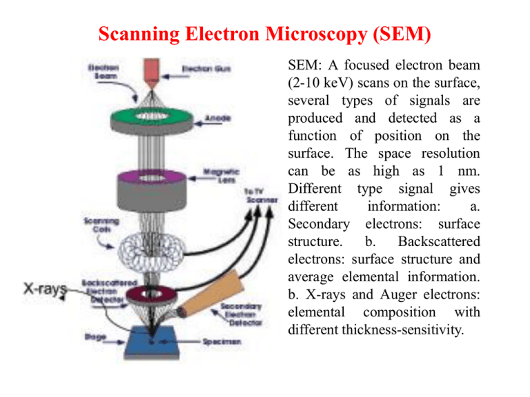
Scanning Electron Microscopy (SEM) SEM: A focused electron beam (2-10 keV) scans on the surface, several types of signals are produced and detected as a function of position on the surface. The space resolution can be as high as 1 nm. Different type signal gives different information: a. Secondary electrons: surface structure. b. Backscattered electrons: surface structure and average elemental information. b. X-rays and Auger electrons: elemental composition with different thickness-sensitivity. The image formation TV screen e-beam The selection of signal Advantages of Using SEM over OM OM SEM Magnification 4x – 1000x 10x – 3000000x Depth of Field 15.5mm – 0.19mm 4mm – 0.4mm Resolution ~ 0.2mm 1-10nm The SEM has a large depth of field, which allows a large amount of the sample to be in focus at one time and produces an image that is a good representation of the three-dimensional sample. The SEM also produces images of high resolution, which means that closely features can be examined at a high magnification. The combination of higher magnification, larger depth of field, greater resolution and compositional and crystallographic information makes the SEM one of the most heavily used instruments in research areas and industries, especially in semiconductor industry. OM SEM Schematic set-up of SEM Topographic contrast arises because SE generation depend on the angle of incidence between the beam and sample. Backscattered Electrons (BSE) BSE yield: h=nBS/nB ~ function of atomic number Z. BSE images show characteristics of atomic number contrast, i.e., high average Z appear brighter than those of low average Z. BSE image from flat surface of an Al (Z=13) and Cu (Z=29) alloy Different surface sensitivity Auger electron and X-ray can be the signal source for SEM and obtain the elemental composition microscopy but with totally different surface sensitvity. Why suitable for high energy e magnetic lens Magnetic lens (solenoid) (Beam diameter) F = -e(v x B) p q Lens formula: 1/f = 1/p + 1/q Demagnification: M = q/p f Bo2 f can be adjusted by changing Bo, i.e., changing the current through coil. TEM Control brightness, convergence binocular screen Control contrast Interpretation of Images bend contour Dislocations loop A buckled region of a thin foil and bend contour occurs where the Bragg condition is locally satisfied. Bent foil image 0.5m Dislocations are readily analyzed and characterized by means of diffraction contrast. Why TEM The uniqueness of TEM is the ability to obtain full morphological (grain size, grain boundary and interface, secondary phase and distribution, defects and their nature, etc.), crystallographic, atomic structural and micro-analytical such as chemical composition (at nm scale), bonding (distance and angle), electronic structure, coordination number data from the sample. TEM is the most efficient and versatile technique for the characterization of materials. It has many mechanism for contrast in TEM for different application purpose. limitation More or less bulk-like information, the sample cannot be too thick, Sample preparation can be difficult. Comparison of OM,TEM and SEM Source of electrons Light source Condenser Magnetic lenses Specimen Objective Projector Eyepiece Specimen CRT Cathode Ray Tube detector OM TEM SEM Principal features of an optical microscope, a transmission electron microscope and a scanning electron microscope, drawn to emphasize the similarities of overall design. PEEM(Photoemission Electron Microscope) Resolution reached < 20 nm PEEM with integral sample stage for precise sample positioning via remote controlled piezodrives. Secondary electrons generated by the incident X-rays are focused by the lenses to form a magnified image of the electron yield distribution emerging from the sample surface. •Topography contrast •Work funktion contrast •Chemical contrast (absorption edges) •Magnetic contrast (magnetic dicchroism) Secondary have relatively long free path length (10nm), very suitable study multilayer Low Energy Electron Microscopy (LEEM) a b a) Si(001) atomic arrangement b) the corresponding diffraction pattern Basically same as PEEM but with e source Green spots Red spots Localized structural information Scanning Probe Microscopy (SPM) 1. Scanning tunneling Microscopy (STM) I = U/d exp(-Kd f1/2) Inverse decay length K (reciprocal of distance for density to fall to K = 2p/h (2me f)1/2 1/e): STM is based on the tunneling current between a metallic tip and the sample surface, which depends on voltage (U), distance d, and work f average of the two work functions of both sides , K is a constant. STM works only with conducting sample ! Tunneling between two metals Without bias tunneling Without bias tunneling Spatial Resolution of STM I = U/d exp(-Kdf1/2) For a typical metal (K = 1 Å), current falls about an order of magnitude for an increase of 1.0 Å in d. very sensitive dependence of tunnel current on d - good "vertical“ resolution. If one metal is sharp tip, most of Itunnel will travel through pinnacle atom good "lateral" resolution How STM works More compact material changes length in applied electric field - 10-4 to 10-7 % length change per V allows < 0.5 Å positioning for in-plane and vertical resolution < 0.05 Å. The image formation I change Constant Height Mode Tip-sample distance fixed variation in Itunnel forms image Fast but only works for flat samples How the scan works height change Itunnel constant by moving tip up and down (feedback circuitry) - z movement becomes image Slower but works for rough surfaces Most common The tip sharpness Sharpness is essential !!! good Etching: a common way - bad + Tip radius < 20 nm !!! NaOH Etched not etched STM Vibration isolation of the STM (SPM) device is very important (spring, eddy current damping magnet assemblies, etc). The vertical resolution is 0.05 Å!! The electric isolation is also important, the tunneling current normally nA – pA. tip spring STM on clean surface and with absorbent Atom-resolved !!! Ag(110) clean surface with step edge O2 covered Ag(110) Image of work function Normal STM mode can not distinguish the change of morphology (height) from work function (see the formula before), however, from the formula , which able to tell the difference. Au on Si(111) line scan of both z and f, the change of z is due to change of work function (where there is Au). Tunneling from tip to substrate Tunneling is current from occupied states of one side to unoccupied states of another side of the STM. The direction of current depends on bias. The current depends the filled or unfilled electron states near the Fermi surface. Between metal tip to semiconductor IV curve: Scanning Tunneling Spectroscopy Unique peak at certain bias When tip is biased negative, one gets information about empty electronic states on surface. When tip is biased positive, one gets information about filled electronic states on surface. With the same height, one record the current as function of bias voltage, in reality this measurement is often plotted as I/V, dI/dV, or d2I/dV2 curves. This kind of plot provides atom-resolved information about local electronic (and even vibrational) structure. Simply one can can do STM at changing bias to resolve "location" of individual electronic states. Manipulation Several methods: - field effect - under influence of high electric field, polarizable molecule or atom can be made to jump from surface to tip or vice versa. - dragging - vdW forces between close tip and adsorbate can be used to drag species. Tip Atomic Force Microscope Cantilever Can work with insulator Soft, flexible (low spring constant) The Force that is experience by the tip is mainly due to Van der Waals force, typically 10-11 to 10-6 N at separation of ~ 1 Å. Working modes Contact Mode (Repulsive Mode): Tip makes a “soft physical” contact with the surface and scan. Repulsive force on tip about 10-6 – 10-8 N. operates in ambient or in liquid. frictional force that will distort the image. Works in two modes: constant force or constant height. non-contact mode (attractive Mode): Tip-surface distance 10-100 Å. Attractive force of 10-12 N. uses AC driven oscillating cantilever (1001000 Hz frequency, 10-100 Å amplitude) to sense the changes in the resonant frequency of a cantilever which reflect changes in the tip-to-sample spacing. Fluid contamination may result in a quite different picture. best for soft or elastic surfaces. least contamination. least destructive. long tip life intermittent contact (tapping) mode: Similar to non-contact using vibrating cantilever except at one extent tip "taps“(barely contact) into contact. The amplitude > 20 Å, the change of the amplitude due to tap will be sensed. Useful for soft surfaces - less prone to external vibration/noise than noncontact, but will not image water layers (pierce). Less destructive than contact AFM and can image rougher samples. Working modes a b c Contact(repulsive) Non-contact (attractive) Tapping a.Sliding the probe tip across surface, heavily influenced by frictional and adhesive forces, which can damage samples and distort image data. b.Sensing Van der Waals attractive forces between surface and probe tip held above surface (50 - 150 Å), low resolution and can also be hampered by the contaminant layer which can interfere with oscillation. c.Tapping the surface with an oscillating probe tip, eliminates frictional forces by intermittently contacting the surface and oscillating with sufficient amplitude to prevent the tip from being trapped by adhesive meniscus forces from the contaminant layer. Fluid contamination Non-contact AFM contact AFM AFM photos Protein Atom-resolved 50 x 50 m NaCl(100) surface using a variant of contact mode UHV AFM – arrow shows defects Creature with mouth More Scanning Probe techniques AFM MFM Lateral Force Microscopy (LFM): measures frictional forces between the probe tip and the sample surface Magnetic Force Microscopy (MFM): measures magnetic gradient and distribution above the sample surface; Electric Force Microscopy (EFM): measures electric field gradient and distribution above the sample surface; Scanning Thermal Microscopy (SThM): measures temperature distribution on the sample surface. Scanning Capacitance Microscopy (SCM): measures carrier (dopant) concentration profiles on semiconductor surfaces. Spin-resolved STM: atom-resolved magnetic microscopy.
