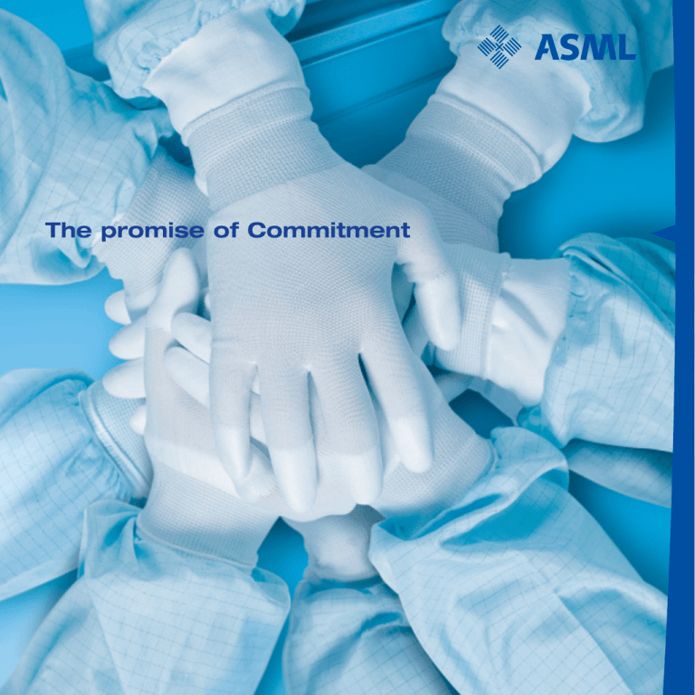
The promise of Commitment
ASML Mission
Providing leading edge imaging solutions
to continuously improve our customers’
global competitiveness
ASML Commitment
Since the company was founded in 1984, the promise
of commitment has been consistent with the values of
ASML. It is the foundation for our relationship with all our
stakeholders: customers, employees, investors, suppliers
and others.
When customers, investors and others relate with our
company, they experience the ASML brand of people,
products and performance. One brand – the promise
of commitment.
ASML’s commitment is to be the industry’s global leader
in semiconductor lithography equipment: the imaging
of nanometric circuit patterns on a silicon wafer, the
material from which integrated circuits are made.
ASML business strategy
Our business strategy is based on technology leadership, customer focus and operational excellence. Simply
stated, ASML is committed to add measurable value
and long-term results to benefit our customers as they
design, produce and price their products.
As technology roadmaps and customer requirements
become more demanding, ASML needs the best talent
available. That is why we’re committed to developing
our people and creating a learning culture. ASML’s
human resource strategy embraces our unique culture
of individual and team commitment that makes
outstanding accomplishments possible.
ASML Technology Leadership
Technology leadership is recognition for those who
are continually at the forefront of the industry. And
ASML has evidence of such leadership. We are the
global market leader, with proof of customer acceptance
for our steppers and advanced Step & Scan systems
that span the industry’s current wavelength technology
for 200 and 300 millimeter wafers alike.
Productivity for ASML customers
We drive technology leadership along the semiconductor
industry roadmap in consultation with existing customers and potential new ones. We seek to satisfy the
needs of different types of chipmakers by customizing
and configuring products to provide premium value
for the owners of ASML lithography systems.
Since 2000, we have offered the industry’s only dualstage wafer imaging system – our TWINSCAN™ platform
– that allows exposure of one wafer while simultaneously
measuring another wafer. Two wafer stages improve
productivity and accuracy.
We pursue world class productivity to benefit every type
of customer: from makers of memory chips and complex
microprocessors to independent device manufacturers
and made-to-order chip contractors. We also form and
maintain strategic alliances with other semiconductor
equipment suppliers, allowing us to offer customers
more complete solutions.
In 2003, we introduced our new immersion lithography
system, a pioneering and promising product that
replaces the air over the wafer with fluid to enhance
focus and shrink line widths. This means opportunities
for making smaller, smarter semiconductors.
ASML Customer Focus
Everyone at ASML is responsible for customer focus.
ASML’s commitment to customers is to develop, install
and support technological tools for volume production.
Doing so enables customers to become better
competitors and make more profit.
Customer focus includes multi-discipline account
management teams. Account managers represent our
customers across every function and business process
at ASML: from marketing and technology to logistics
and customer support.
We track and treat levels of customer satisfaction using
our own systematic methods. Customers also provide
ratings based on their own criteria. Independent industry
surveys of customer satisfaction compare ASML with
large suppliers of all types of chipmaking gear.
Superior value of ASML tools
We engage customers in very early stages of technology
development. We listen to their needs surrounding
product introduction and volume utilization. Together,
we create a dynamic and shared roadmap that begins
with a customer need and ends with a customer
solution.
ASML offers superior value for owners of ASML
systems. It allows each customer to operate their chip
fabrication facilities – anywhere in the world – with
highest productivity. Customers calculate their return
on capital employed in semiconductor fabrication
facilities. They assess ASML’s added value.
When customers are satisfied, they have the confidence
to commit to capital expenditures: customers repeat
purchases of ASML lithography systems and buy
additional products and services.
ASML Operational Excellence
Inside ASML, we sharpen our strategic focus through
the work of multiple cross-functional process improvement teams. From an operational perspective, these
process improvement teams are striving to streamline
and integrate main business processes such as new
product introduction, acquisition of orders from
customers, fulfillment of orders, and our post-delivery
support and services.
ASML Value Sourcing
ASML’s business strategy includes outsourcing the
majority of components and subassemblies that make
up our lithography products. We work in partnership
with suppliers, jointly operating a strategy known as
Value Sourcing. It is based on the QLTC principle that
stands for quality, logistics, technology and total cost.
With ASML Value Sourcing, we strive to attain flexibility, best-of-breed contributions and cost savings.
It exemplifies mutual commitment, alongside shared
risk and reward.
Improving ASML’s results
Operational excellence is also a strategic pillar that
supports reduction of fixed and variable costs. Doing
so at once increases operating profit and generates
cash from working capital.
Operational excellence enhances efficiencies and
effectiveness in many ways such as research and
development; selling, general and administrative
expenses; manufacturing and other activities.
All in all, operational excellence strengthens ASML’s
ability to offer customers a range of technological
and system choices at the right time in different
semiconductor market segments.
About ASML
ASML is the world’s leading provider of lithography
systems for the semiconductor industry, manufacturing
complex machines critical to the production of
integrated circuits or chips.
ASML technology transfers circuit patterns onto
silicon wafers to make every kind of chip used today
and tomorrow. As digital products, such as PCs and
mobile phones, become more pervasive, the technology
behind chip manufacturing becomes more advanced.
With each generation of chips, personal and business
products become smaller, lighter, faster, more powerful,
more precise, more reliable and easier to use.
Most of the major global semiconductor manufacturers
are ASML customers. We are committed to providing
customers with the right technology that is productionready at the right time. Doing so enables our customers
and their customers to sustain their competitive edge
in the marketplace.
ASML operates in 14 countries and over 50 service
locations. We have experts located at customer sites,
backed by a global pool of ASML engineers and other
professionals.
ASML Special Applications focuses on solutions for
application markets, and has also developed expertise
to certify and relaunch previously used ASML equipment
into the market. ASML MaskTools provides innovative
mask technologies and software products that extend
the limits of optical lithography for chip manufacturing.
ASML Optics is an extreme precision optical foundry
offering design-to-image solutions for the semiconductor
and optical manufacturing industries.
ASML’s corporate headquarters is in Veldhoven, the
Netherlands. The company has lithography research,
development and manufacturing operations in Wilton,
Connecticut and Veldhoven, the Netherlands.
Technology development centers and training and
application facilities are located in Asia, Europe and
the United States.
ASML is traded on Euronext Amsterdam and NASDAQ
under the symbol ASML.
Commitment to Each Other
Race ahead with TWINSCAN
The world’s only dual wafer-stage lithography system
ASML TWINSCAN lithography systems deliver the
highest productivity at the limits of optical lithography.
TWINSCAN is the semiconductor industry’s only
platform that combines world-class measurement
accuracy with simultaneous, nonstop wafer imaging.
How? It is the world’s only semiconductor imaging
system with dual wafer-stages.
ASML Contact
Corporate
Headquarters
De Run 6501
5504 DR Veldhoven
P.O. Box 324
5500 AH Veldhoven
The Netherlands
phone: +31 40 268 3000
www.asml.com
© 2004, ASML Holding
N.V. All Rights Reserve
U.S. main offices
8555 South River Parkway
Tempe, AZ 85284 U.S.A.
phone: +1 480 383 4422
77 Danbury Road
Wilton, CT 06897 U.S.A.
phone: +1 203 761 4000
Asia main office
Suite 603, 6/F
One International
Finance Center
1, Harbour View Street
Central,
Hong Kong, SAR
phone: +852 2295 1168
Corporate
Communications
phone: +31 40 268 4941
e-mail:
corpcom@asml.com
Investor
Relations
phone: +31 40 268 3938
e-mail:
investor.relations@asml.com
