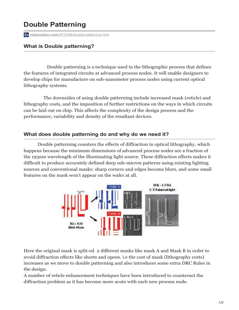
Double Patterning vlsijunction.com/2015/08/double-patterning.html What is Double patterning? Double patterning is a technique used in the lithographic process that defines the features of integrated circuits at advanced process nodes. It will enable designers to develop chips for manufacture on sub-nanometer process nodes using current optical lithography systems. The downsides of using double patterning include increased mask (reticle) and lithography costs, and the imposition of further restrictions on the ways in which circuits can be laid out on chip. This affects the complexity of the design process and the performance, variability and density of the resultant devices. What does double patterning do and why do we need it? Double patterning counters the effects of diffraction in optical lithography, which happens because the minimum dimensions of advanced process nodes are a fraction of the 193nm wavelength of the illuminating light source. These diffraction effects makes it difficult to produce accurately defined deep sub-micron patterns using existing lighting sources and conventional masks: sharp corners and edges become blurs, and some small features on the mask won’t appear on the wafer at all. Here the original mask is split-ed 2 different masks like mask A and Mask B in order to avoid diffraction effects like shorts and opens. i.e the cost of mask (lithography costs) increases as we move to double patterning and also introduces some extra DRC Rules in the design. A number of reticle enhancement techniques have been introduced to counteract the diffraction problem as it has become more acute with each new process node. 1/2 Phase-shift masks: were introduced at the 180nm process node. They alter the phase of the light passing through some areas of the mask, changing the way it is diffracted and so reducing the defocusing effect of mask dimensions that are less than the wavelength of the illuminating light. The downside of using phase-shift techniques is that the masks are more difficult and expensive to make. Optical-proximity correction (OPC) techniques work out how to distort the patterns on a mask to counter diffraction effects, for example by adding small ‘ears’ to the corners of a square feature on the mask so that they remain sharply defined on the wafer. The technique introduces layout restrictions, has a computational cost in design, and means that it takes longer and costs more to make the corrected masks. 2/2


