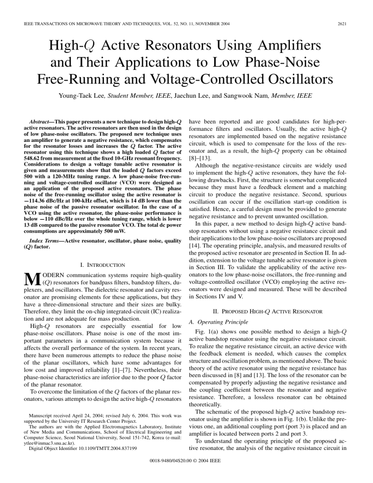
IEEE TRANSACTIONS ON MICROWAVE THEORY AND TECHNIQUES, VOL. 52, NO. 11, NOVEMBER 2004 2621 High-Q Active Resonators Using Amplifiers and Their Applications to Low Phase-Noise Free-Running and Voltage-Controlled Oscillators Young-Taek Lee, Student Member, IEEE, Jaechun Lee, and Sangwook Nam, Member, IEEE Abstract—This paper presents a new technique to design highactive resonators. The active resonators are then used in the design of low phase-noise oscillators. The proposed new technique uses an amplifier to generate a negative resistance, which compensates factor. The active for the resonator losses and increases the resonator using this technique shows a high loaded factor of 548.62 from measurement at the fixed 10-GHz resonant frequency. Considerations to design a voltage tunable active resonator is given and measurements show that the loaded factors exceed 500 with a 120-MHz tuning range. A low phase-noise free-running and voltage-controlled oscillator (VCO) were designed as an application of the proposed active resonators. The phase noise of the free-running oscillator using the active resonator is 114.36 dBc/Hz at 100-kHz offset, which is 14 dB lower than the phase noise of the passive resonator oscillator. In the case of a VCO using the active resonator, the phase-noise performance is below 110 dBc/Hz over the whole tuning range, which is lower 13 dB compared to the passive resonator VCO. The total dc power consumptions are approximately 500 mW. Index Terms—Active resonator, oscillator, phase noise, quality ( ) factor. I. INTRODUCTION M ODERN communication systems require high-quality ( ) resonators for bandpass filters, bandstop filters, duplexers, and oscillators. The dielectric resonator and cavity resonator are promising elements for these applications, but they have a three-dimensional structure and their sizes are bulky. Therefore, they limit the on-chip integrated-circuit (IC) realization and are not adequate for mass production. resonators are especially essential for low Highphase-noise oscillators. Phase noise is one of the most important parameters in a communication system because it affects the overall performance of the system. In recent years, there have been numerous attempts to reduce the phase noise of the planar oscillators, which have some advantages for low cost and improved reliability [1]–[7]. Nevertheless, their phase-noise characteristics are inferior due to the poor factor of the planar resonator. To overcome the limitation of the factors of the planar resonators, various attempts to design the active high- resonators Manuscript received April 24, 2004; revised July 6, 2004. This work was supported by the University IT Research Center Project. The authors are with the Applied Electromagnetics Laboratory, Institute of New Media and Communications, School of Electrical Engineering and Computer Science, Seoul National University, Seoul 151-742, Korea (e-mail: ytlee@inmac3.snu.ac.kr). Digital Object Identifier 10.1109/TMTT.2004.837199 have been reported and are good candidates for high-performance filters and oscillators. Usually, the active highresonators are implemented based on the negative resistance circuit, which is used to compensate for the loss of the resonator and, as a result, the high- property can be obtained [8]–[13]. Although the negative-resistance circuits are widely used to implement the high- active resonators, they have the following drawbacks. First, the structure is somewhat complicated because they must have a feedback element and a matching circuit to produce the negative resistance. Second, spurious oscillation can occur if the oscillation start-up condition is satisfied. Hence, a careful design must be provided to generate negative resistance and to prevent unwanted oscillation. In this paper, a new method to design high- active bandstop resonators without using a negative resistance circuit and their applications to the low phase-noise oscillators are proposed [14]. The operating principle, analysis, and measured results of the proposed active resonator are presented in Section II. In addition, extension to the voltage tunable active resonator is given in Section III. To validate the applicability of the active resonators to the low phase-noise oscillators, the free-running and voltage-controlled oscillator (VCO) employing the active resonators were designed and measured. These will be described in Sections IV and V. II. PROPOSED HIGH- ACTIVE RESONATOR A. Operating Principle Fig. 1(a) shows one possible method to design a highactive bandstop resonator using the negative resistance circuit. To realize the negative resistance circuit, an active device with the feedback element is needed, which causes the complex structure and oscillation problem, as mentioned above. The basic theory of the active resonator using the negative resistance has been discussed in [8] and [13]. The loss of the resonator can be compensated by properly adjusting the negative resistance and the coupling coefficient between the resonator and negative resistance. Therefore, a lossless resonator can be obtained theoretically. The schematic of the proposed high- active bandstop resonator using the amplifier is shown in Fig. 1(b). Unlike the previous one, an additional coupling port (port 3) is placed and an amplifier is located between ports 2 and port 3. To understand the operating principle of the proposed active resonator, the analysis of the negative resistance circuit in 0018-9480/04$20.00 © 2004 IEEE 2622 IEEE TRANSACTIONS ON MICROWAVE THEORY AND TECHNIQUES, VOL. 52, NO. 11, NOVEMBER 2004 Q Fig. 1. High- active bandstop resonator using: (a) the negative resistance circuit. (b) The amplifier. Fig. 3. Calculated equivalent: (a) j0 Fig. 2. Simulation setup to calculate the equivalent negative resistance seen from the resonator. Fig. 1(a) should be performed. Basically, the negative resistance plays a role of reflection-type amplification of the signal, which seen from port 2 means that the reflection coefficient to the negative resistance circuit exceeds one near the resonant frequency. The active resonator proposed in this paper shows similar operation. A power is injected into port 1 and coupled to ports 2 and 3. The power from port 3 is then amplified and injected to port 2 in the opposite direction, as shown in Fig. 1(b). By of the transmission lines located adjusting the phases at the two coupling ports, is larger than one, has negative resistance. In conclusion, which suggests that the high- active resonator can be designed simply using the amplifier without the complicated negative resistance circuit. B. Analysis The equivalent negative resistance can be calculated from the linear circuit simulation. Fig. 2 shows the simulation setup to calculate the negative resistance. Note that there are three ports (i.e., ports 1, A, and B) in this setup, and the dual-power sampler, which is an ideal device, is included in the active resonator circuit. The dual-power sampler j and (b) Z . and plays a role of sampling the power from the resonator , and they are equal to and power to the resonator , respectively. Therefore, the equivalent reflection coefficient seen from the resonator and input impedance can be calculated using the following equation: (1) Fig. 3 shows the equivalent and resulting input impedance obtained from the circuit simulation. It is is 5 dB and is at the calculated that resonant frequency. One may doubt that there is a possibility of oscillation because the amplifier is located in a closed loop. However, the coupling coefficient between ports 2 and 3 in Fig. 1(b) is very weak (below 10 dB), which indicates that the loop gain of the closed loop is less than unity at whole frequency bands, as shown in Fig. 4. Therefore, no oscillation can occur. The loop gains must be checked in other values of port-1 terminations such as reacand tive terminations. Since the transmission coefficients in Fig. 1(b) are very weak (below 10 dB), the port-1 termination does not affect the loop gain characteristics seriously. in Fig. 1(b) is Actually the variance of the magnitude of within 2 dB when port 1 is terminated in reactive impedance. From the circuit simulation, it was found that the loop gains LEE et al.: HIGH- ACTIVE RESONATORS USING AMPLIFIERS 2623 Fig. 6. Circuit diagram of the proposed voltage tunable highresonator. Fig. 4. Characteristics of the loop gain. Port 1 is terminated in 50 active . Fig. 7. Frequency response tuning range is 120 MHz. Fig. 5. Frequency responses (0) of the passive resonator (measurement), active resonator (simulation and measurement), and active resonator when the bias is off (measurement). were slightly increased in the case of reactive port-1 terminations, but also less than unity. C. Fabrication and Measurements The active resonator was fabricated using a Teflon substrate of 0.504-mm thickness and the dielectric constant of 2.52 with the hybrid technique. The TC 2381 medium power device was used as an amplifier to be operated in the linear region. The simulated and measured return-loss results of the proposed active bandstop resonator are in good agreement, as shown in Fig. 5. The loaded factor from the measurement is calculated to be 548.62. For comparison, a passive resonator strongly coupled to the microstrip line is also fabricated and measured. The measured result of the passive resonator is also factor is calculated to be shown in Fig. 5 and the loaded 65.72. III. VOLTAGE TUNABLE HIGH- Q ACTIVE RESONATOR Fig. 6 shows the circuit diagram of the voltage tunable highactive resonator. The varactor diode is attached to change the resonant frequency of the resonator. The MA 46H120 was used (0) of the voltage tunable active resonator. The and its capacitance is varied from 0.9 to 0.2 pF for control voltages of 1–10 V. The operating principle and design procedure of this voltage tunable active resonator are identical to those of the fixed frequency active resonator. The voltage tunable active resonator based on the negative resistance circuit can be implemented just by attaching the varactor diode in Fig. 1(a). Since the negative resistance in Fig. 1(a) is not an ideal device in reality, its value is not constant versus frequency. Moreover, the negative resistance does not dependent on the varactor diode control voltages. This indicates that the performance of the voltage tunable active resonator using negative resistance can be degraded varying the resonant frequency. In some cases, the oscillation can occur when the negative resistance circuit is modified to fulfill the desired performances at the whole tuning range. On the other hand, in the case of the proposed voltage tunable active resonator in Fig. 6, the varactor diode control voltages can at the resonant frechange both the resonant frequency and quency. This arises from the fact that the characteristics of the closed loop are changed depending on the resonant frequency. Therefore, it is possible to achieve high input reflection coeffiand high loaded ’s at the whole tuning ranges. cients Fig. 7 shows the measured characteristics of the voltage tunable active resonator. The loaded is larger than 500 at the all resonant frequencies. 2624 IEEE TRANSACTIONS ON MICROWAVE THEORY AND TECHNIQUES, VOL. 52, NO. 11, NOVEMBER 2004 Fig. 8. Schematics of the: (a) free-running ARO and (b) VCARO. Fig. 9. Measured phase-noise characteristics of the ARO and PRO at 100-kHz offset. (a) Depending on the drain bias voltages (V = 0:4 V). (b) Depending on the gate bias voltages (V = 1 V). 0 IV. DESIGN OF OSCILLATORS USING HIGH- ACTIVE RESONATORS The schematics of the free-running active resonator oscillator (ARO) and the voltage-controlled active resonator oscillator (VCARO) are shown in Fig. 8(a) and (b), respectively. The active devices for the oscillators are NE 32584 high electronmobility transistor (HEMT) devices and they were designed using the nonlinear simulation approach [15]. The oscillation frequency of the free-running ARO is 10 GHz, which is the resonant frequency of the active resonator. In the case of a VCARO, the oscillation frequencies are changed according to the control voltages of the varactor diode, as described in Section III. The free-running passive resonator oscillator (PRO) and the voltage-controlled passive resonator oscillator (VCPRO) were also fabricated to compare the factors and resulting phasenoise performances. Note that the source and drain circuits of the oscillators using the passive resonators are identical to those of the oscillators using the active resonators. V. MEASURED RESULTS OF THE AROs A. Free-Running Oscillators The phase-noise characteristics of the free-running ARO and PRO were measured using the Agilent E4448A spectrum analyzer. Fig. 9 depicts the measured phase-noise results of these two oscillators depending on the bias voltages. The phase noises Fig. 10. Measured oscillation frequency deviation (VSWR = 1:0933). of the ARO are lower than those of the PRO by 14–15 dB. The output powers of the ARO and PRO are 10.74 and 6.19 dBm, V and V. respectively, at To demonstrate the high-quality property of the ARO and compare it with the factor of the PRO, the pulling figure must be measured [16]. The pulling figure means the maximum oscillation frequency deviation for a load mismatch of all phases. In the experiment, the pulling figures of these two oscillators were measured for the load voltage standing wave ratio (VSWR) LEE et al.: HIGH- Fig. 11. ACTIVE RESONATORS USING AMPLIFIERS Output spectrum of the ARO (V = 00:4 V, V = 1 V). 2625 Fig. 14. Output spectrum of the VCARO (V = 00:4 V, V = 1 V). TABLE I COMPARISON BETWEEN THIS STUDY AND OTHER PLANAR TECHNOLOGIES Fig. 12. Tuning ranges of the VCARO and VCPRO versus the control voltages of the varactor diode. of the external ’s is 5.59 and 14.9-dB phase-noise improvement is expected. This is in good agreement with the measured phase-noise results. The output spectrum of the ARO is illustrated in Fig. 11 and it shows 114.36 dBc/Hz at 100-kHz offset. B. VCOs Fig. 13. Measured phase-noise characteristics of the VCARO and VCPRO versus the control voltages of the varactor diode (V = 0:4 V, V = 1 V). 0 of 1.0993. Under this condition, the maximum oscillation frequency deviations of the ARO and PRO are 0.78 and 4.36 MHz, factor as shown in Fig. 10. This gives rise to the external of 1211 and 216.6, respectively. This indicates that the ratio Fig. 12 shows the measured oscillation frequencies versus the varactor control voltages. The tuning ranges of the VCARO and VCPRO are 107 and 135 MHz, respectively. The measured phase-noise performances are shown in Fig. 13. It should be noted that the phase noises of the VCARO are below 110 dBc/Hz at 100-kHz offset for the whole tuning range due to the good performance of the voltage tunable active resonator. To the best of our knowledge, it is lower or comparable to the phase-noise performances in [3] and [7], which used low-noise silicon devices for VCOs at -band. Fig. 14 shows the output spectrum of the VCARO. 2626 IEEE TRANSACTIONS ON MICROWAVE THEORY AND TECHNIQUES, VOL. 52, NO. 11, NOVEMBER 2004 Table I shows the comparison of oscillator phase-noise performances between the proposed ARO, VCARO, and other oscillator technologies. VI. CONCLUSION A new design technique of the high- active resonators using amplifiers for planar structures has been proposed. It overcomes the difficulties of the conventional active resonators using negative-resistance circuits such as design complexity, oscillation, and hard tunable problems. An analysis procedure to calculate the equivalent negative resistance using computer-aided design (CAD) has been discussed. A fixed and voltage tunable active resonators using the proposed technique has been designed and their loaded factors have been shown to be larger than 500 from measurements. To demonstrate the applicability of the proposed active resonators, the phase-noise performances of the free-running oscillators and VCOs employing the active resonators have been measured. Due to the high- factors of the proposed active resonators, the active resonators oscillators exhibit low phasenoise results, 114.36 dBc/Hz for the free-running oscillator and below 110 dBc/Hz for the VCO at 100-kHz offset. In addition, it is expected that the proposed active resonator scheme can be applied to other circuits such as bandpass filters and parallel-feedback oscillators. REFERENCES [1] Y.-T. Lee, J.-S. Lim, J.-S. Park, D. Ahn, and S. Nam, “A novel phase noise reduction technique in oscillators using defected ground structure,” IEEE Microwave Wireless Comp. Lett., vol. 12, pp. 39–41, Feb. 2002. [2] Y.-T. Lee, J.-S. Lim, C.-S. Kim, D. Ahn, and S. Nam, “A compact-size microstrip spiral resonator and its application to microwave oscillator,” IEEE Microwave Wireless Comp. Lett., vol. 12, pp. 375–377, Oct. 2002. [3] L. Dussopt, D. Guillois, and G. M. Rebeiz, “A low phase noise silicon 9 GHz VCO and 18 GHz push–push oscillator,” in IEEE MTT-S Int. Microwave Symp. Dig., vol. 2, June 2002, pp. 695–698. [4] W.-C. Lee, S.-C. Lin, and C.-K. C. Tzuang, “Planar realization of low phase noise 15/30 GHz oscillator/doubler using surface mount transistors,” IEEE Microwave Wireless Comp. Lett., vol. 13, pp. 10–12, Jan. 2003. [5] Y. Cassivi and K. Wu, “Low cost microwave oscillator using substrate integrated wavegiude cavity,” IEEE Microwave Wireless Comp. Lett., vol. 13, pp. 48–50, Feb. 2003. [6] L.-H. Hsieh and K. Chang, “High-efficiency piezoelectric-transducertuned feedback microstrip ring-resonator oscillators operating at high resonant frequencies,” IEEE Trans. Microwave Theory Tech., vol. 51, pp. 1141–1145, Apr. 2003. [7] A. P. S. Khanna, E. Topacio, E. Gane, and D. Elad, “Low jitter silicon bipolar based VCO’s for applications in high speed optical communication systems,” in IEEE MTT-S Int. Microwave Symp. Dig., vol. 3, May 2001, pp. 1567–1570. [8] C.-Y. Chang and T. Itoh, “Microwave active filters based on coupled negative resistance method,” IEEE Trans. Microwave Theory Tech., vol. 38, pp. 1879–1884, Dec. 1990. [9] Y. Yamamoto, K. Kawasaki, and T. Itoh, “A MESFET-controlled -band active bandpass filter,” IEEE Microwave Guided Wave Lett., vol. 1, pp. 110–111, May 1991. X [10] J. Lin and T. Itoh, “Tunable active filters using three-terminal MESFET varactor,” in IEEE MTT-S Int. Microwave Symp. Dig., vol. 2, May 1992, pp. 921–924. [11] Y.-H. Cho, S.-C. Hong, and Y.-S. Kwon, “A low-power monolithic GaAs FET bandpass filter based on negative resistance technique,” IEEE Microwave Guided Wave Lett., vol. 8, pp. 161–163, Apr. 1998. [12] Y. Yamamoto, Y. Imon, S. Mikumo, and M. Katsuragi, “Tuning a bandpass filter by optical control of a negative-resistance circuit,” IEEE Trans. Microwave Theory Tech., vol. 46, pp. 2006–2010, Dec. 1998. [13] J. Lee, Y.-T. Lee, and S. Nam, “A phase noise reduction technique in microwave oscillator using high- active filter,” IEEE Microwave Wireless Comp. Lett., vol. 12, pp. 426–428, Nov. 2002. [14] Y.-T. Lee, J. Lee, and S. Nam, “New planar high- active resonator and its application to low phase noise oscillators,” in IEEE MTT-S Int. Microwave Symp. Dig., vol. 3, June 2004, pp. 2007–2010. [15] M.-Q. Lee, S.-J. Yi, S. Nam, Y. Kwon, and K.-W. Yeom, “High efficiency harmonic loaded oscillator with low bias using a nonlinear design approach,” IEEE Trans. Microwave Theory Tech., vol. 47, pp. 1670–1679, Sept. 1999. [16] J. Obregon and A. P. S. Khanna, “Exact derivation of the nonlinear negative-resistance oscillator pulling figure,” IEEE Trans. Microwave Theory Tech., vol. MTT-30, pp. 1109–1111, July 1982. Q Q Young-Taek Lee (S’00) was born in Seoul, Korea, on February 8, 1975. He received the B.S., M.S., and Ph.D. degrees in electrical engineering from the Seoul National University, Seoul, Korea, in 1998, 2000, and 2004, respectively. His research interests include the design and analysis of the high- resonators and low phase-noise oscillators for planar structures and applications of defected ground structures to microwave and millimeter-wave circuits. Q Jaechun Lee was born in Seoul, Korea, on October 27, 1973. He received the B.S. degree in electrical engineering from Soongsil University, Seoul, Korea, in 2000, the M.S. degree in electrical engineering from the Seoul National University, Seoul, Korea, in 2002, and is currently working toward the Ph.D. degree at Seoul National University. His research interests include the dynamics of coupled oscillators and high-efficiency power-combining techniques. Sangwook Nam (S’87–M’88) received the B.S. degree from Seoul National University, Seoul, Korea, in 1981, the M.S. degree from the Korea Advanced Institute of Science and Technology, Seoul, Korea, in 1983, and the Ph.D. degree from The University of Texas at Austin, in 1989, all in electrical engineering. From 1983 to 1986, he was a Researcher with the Gold Star Central Research Laboratory, Seoul, Korea. Since 1990, he was been with Seoul National University, where he is currently a Professor with the School of Electrical Engineering and Computer Science. His research interests include analysis/design of electromagnetic (EM) structures, antennas, and microwave active/passive circuits.
