Semiconductor Devices Assignment: Conductivity & Fermi Level
advertisement
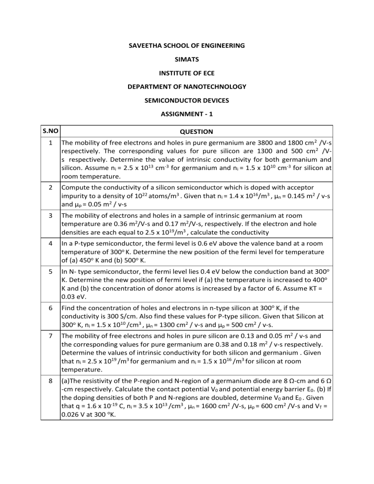
SAVEETHA SCHOOL OF ENGINEERING SIMATS INSTITUTE OF ECE DEPARTMENT OF NANOTECHNOLOGY SEMICONDUCTOR DEVICES ASSIGNMENT - 1 S.NO QUESTION 1 The mobility of free electrons and holes in pure germanium are 3800 and 1800 cm 2 /V-s respectively. The corresponding values for pure silicon are 1300 and 500 cm2 /Vs respectively. Determine the value of intrinsic conductivity for both germanium and silicon. Assume ni = 2.5 x 1013 cm-3 for germanium and ni = 1.5 x 1010 cm-3 for silicon at room temperature. 2 Compute the conductivity of a silicon semiconductor which is doped with acceptor impurity to a density of 1022 atoms/m3 . Given that ni = 1.4 x 10¹⁶/m3 , μn = 0.145 m2 / v-s and μp = 0.05 m2 / v-s 3 The mobility of electrons and holes in a sample of intrinsic germanium at room temperature are 0.36 m2/V-s and 0.17 m2/V-s, respectively. If the electron and hole densities are each equal to 2.5 x 10¹⁹/m3 , calculate the conductivity 4 In a P-type semiconductor, the fermi level is 0.6 eV above the valence band at a room temperature of 300o K. Determine the new position of the fermi level for temperature of (a) 450o K and (b) 500o K. 5 In N- type semiconductor, the fermi level lies 0.4 eV below the conduction band at 300o K. Determine the new position of fermi level if (a) the temperature is increased to 400o K and (b) the concentration of donor atoms is increased by a factor of 6. Assume KT = 0.03 eV. 6 Find the concentration of holes and electrons in n-type silicon at 300o K, if the conductivity is 300 S/cm. Also find these values for P-type silicon. Given that Silicon at 300o K, ni = 1.5 x 10¹⁰ /cm3 , μn = 1300 cm2 / v-s and μp = 500 cm2 / v-s. 7 The mobility of free electrons and holes in pure silicon are 0.13 and 0.05 m2 / v-s and the corresponding values for pure germanium are 0.38 and 0.18 m2 / v-s respectively. Determine the values of intrinsic conductivity for both silicon and germanium . Given that ni = 2.5 x 10¹⁹ /m3 for germanium and ni = 1.5 x 10¹⁶ /m3 for silicon at room temperature. 8 (a)The resistivity of the P-region and N-region of a germanium diode are 8 Ω-cm and 6 Ω -cm respectively. Calculate the contact potential V0 and potential energy barrier E0. (b) If the doping densities of both P and N-regions are doubled, determine V0 and E0 . Given that q = 1.6 x 10⁻¹⁹ C, ni = 3.5 x 10¹³ /cm3 , μn = 1600 cm2 /V-s, μp = 600 cm2 /V-s and VT = 0.026 V at 300 oK.
