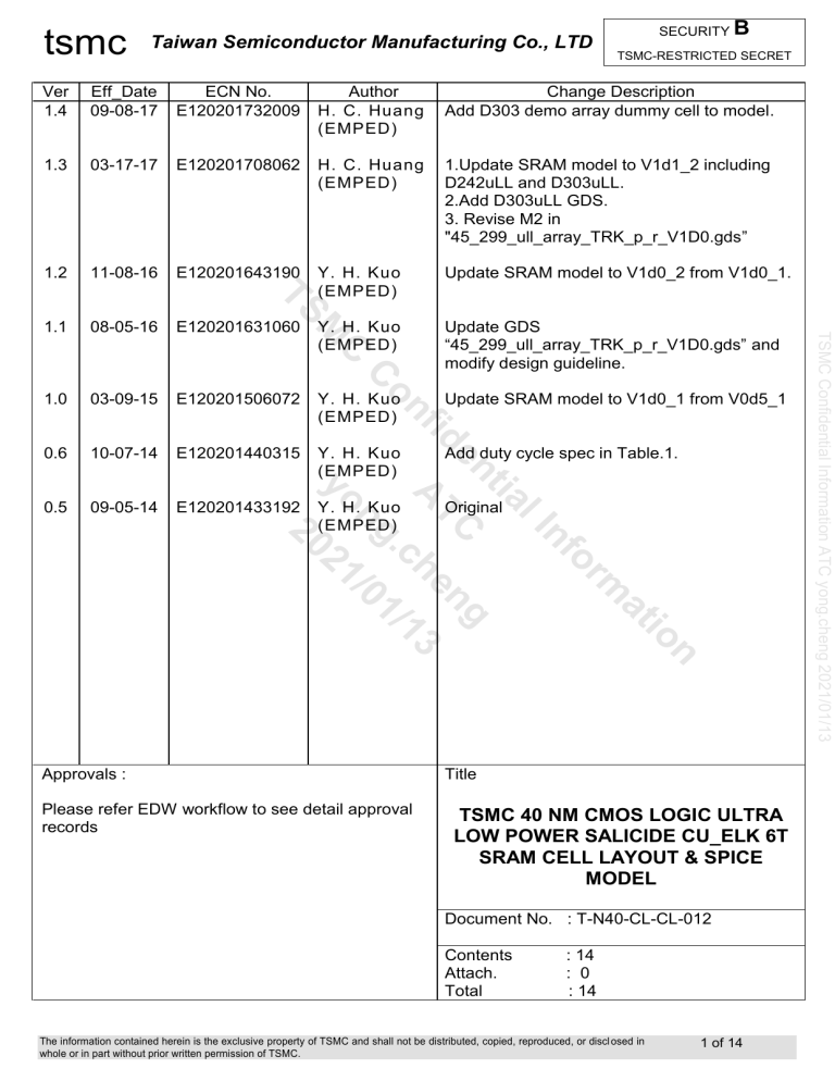
tsmc Taiwan Semiconductor Manufacturing Co., LTD SECURITY B TSMC-RESTRICTED SECRET ECN No. E120201732009 Author H. C. Huang (EMPED) Change Description Add D303 demo array dummy cell to model. 1.3 03-17-17 E120201708062 H. C. Huang (EMPED) 1.Update SRAM model to V1d1_2 including D242uLL and D303uLL. 2.Add D303uLL GDS. 3. Revise M2 in "45_299_ull_array_TRK_p_r_V1D0.gds” 1.2 11-08-16 E120201643190 Y. H. Kuo (EMPED) Update SRAM model to V1d0_2 from V1d0_1. 1.1 08-05-16 E120201631060 Y. H. Kuo (EMPED) Update GDS “45_299_ull_array_TRK_p_r_V1D0.gds” and modify design guideline. 1.0 03-09-15 E120201506072 Y. H. Kuo (EMPED) Update SRAM model to V1d0_1 from V0d5_1 0.6 10-07-14 E120201440315 Y. H. Kuo (EMPED) Add duty cycle spec in Table.1. 0.5 09-05-14 E120201433192 C A n io at m or nf lI tia g en TC en fid h 13 on C yo Original .c ng 1/ /0 21 20 Y. H. Kuo (EMPED) Approvals : Please refer EDW workflow to see detail approval records Title TSMC 40 NM CMOS LOGIC ULTRA LOW POWER SALICIDE CU_ELK 6T SRAM CELL LAYOUT & SPICE MODEL Document No. : T-N40-CL-CL-012 Contents Attach. Total : 14 : 0 : 14 The information contained herein is the exclusive property of TSMC and shall not be distributed, copied, reproduced, or discl osed in whole or in part without prior written permission of TSMC. 1 of 14 TSMC Confidential Information ATC yong.cheng 2021/01/13 Eff_Date 09-08-17 M TS Ver 1.4 tsmc Confidential – Do Not Copy Document No. : T-N40-CL-CL-012 Version : 1.4 LEGAL NOTICE FOR SRAM-RELATED RELEASE What is confidential? All information contained in this release package (not limited to this report), and any information extracted therefrom, is the proprietary and confidential information of TSMC. Information such as LAYOUT, DIMENSION, PERFORMANCE AND POWER DATA, is strictly confidential, and may not be disclosed to another third party without TSMC’s prior written consent. C n io at m or nf lI tia g en TC en fid h 13 on C A yo Is modification permitted? It is also important that you understand that any modification without due consideration, and without support of silicon data could cause severe problems at the design level or at the silicon level. Any modification of the SRAM related information, including but not limited to the SRAM bitcell, is therefore strictly prohibited and require TSMC’s prior written consent. Usage of modified SRAM bitcells must follow the same confidentiality and usage limitations as unmodified SRAM bitcells. .c ng 1/ /0 21 20 The information contained herein is the exclusive property of TSMC and shall not be distributed, copied, reproduced, or disclosed in whole or in part without prior written permission of TSMC. 2 of 14 TSMC Confidential Information ATC yong.cheng 2021/01/13 M TS What are the usage limitations? Any use of the released information shall be in strict accordance with Nondisclosure Agreement and the Cell License Agreement (or TSMC Master Technology License Agreement) between your company and TSMC, and may only be used for products, designs or projects for tape-out and manufacture at TSMC. tsmc Confidential – Do Not Copy Document No. : T-N40-CL-CL-012 Version : 1.4 TSMC 40 NM CMOS LOGIC ULTRA LOW POWER SALICIDE CU_ELK 6T SRAM CELL LAYOUT & SPICE MODEL It includes 1. Introduction ; 2. Special concern for SRAM ; 3. Layout Guideline ; 4. Unit cell: Dummy , Strapping & B oundary cells ; GDS files ; model name 5. CAD layers; 6. SPICE models; 7. Demo array GDS file ; 8. Design guideline ; 9. LVL guideline ; 10. Redundancy C on 2. SPECIAL CONCERN FOR SRAM ..................................................................................................................................... 5 n io at m or nf lI tia g en TC en fid h 13 3. LAYOUT GUIDELINE ......................................................................................................................................................... 6 4. BASIC GDS INFORMATION: ........................................................................................................................................ 9 A yo 5. CAD LAYER MAPPING .................................................................................................................................................... 11 ng 20 6. SPICE MODELS ............................................................................................................................................................... 13 .c 21 7. BITCELL DEMO ARRAY GDS FILE ................................................................................................................................ 13 /0 8. DESIGN GUIDELINE ........................................................................................................................................................ 13 1/ 9. SRAM CELL IP TAG GUIDELINE .................................................................................................................................... 14 10. REDUNDANCY ............................................................................................................................................................... 14 The information contained herein is the exclusive property of TSMC and shall not be distributed, copied, reproduced, or disclosed in whole or in part without prior written permission of TSMC. 3 of 14 TSMC Confidential Information ATC yong.cheng 2021/01/13 C M TS 1. INTRODUCTION ................................................................................................................................................................ 4 tsmc Confidential – Do Not Copy Document No. : T-N40-CL-CL-012 Version : 1.4 1. Introduction 6T Single port SRAM Cell 2017.02.23 Bitcell Version Model Version V1D1_2 .c ng 1/ /0 21 20 45_299_ull_array_p_V1D0.gds 0.9V +/- 10% 1.0V +/- 10% 1.1V +/- 10% 0.6V 0.6V 0.6V -40C~85C (~125C) -40C~85C (~125C) -40C~85C (~125C) 180mV 90mV 0mV 0V (~40mV) 0V (~40mV) 0V (~40mV) < 2Mb A Filename Voltage range Static data retention Temp. Write assist Vccmin Read assist Vccmin Memory density yo Official Release Date & Purpose Cell 2017.02.23 Bitcell Version Official Release HD SP (ULL) 299 V1D0 n io at m or nf lI tia g en TC en fid h 13 on C Date & Purpose 6T Single port SRAM HC SP (ULL) 303 V1D0 Model Version V1D1_2 Filename Voltage range Static data retention Temp. Write assist Vccmin Read assist Vccmin Memory density 45_303_ull_array_p_V1D0.gds 0.9V +/- 10% 1.0V +/- 10% 1.1V +/- 10% 0.6V 0.6V 0.6V -40C~85C (~125C) -40C~85C (~125C) -40C~85C (~125C) 130mV 40mV 0mV 0V (~40mV) 0V (~40mV) 0V (~40mV) < 2Mb * : If the memory size is >2Mb, please contact tsmc Reliability and SRAM team for suggestion in reliability, Read Assist/Write Assist, voltage usage profile, duty cycle, temperature and Vmin spec. [Table.1] Summary of TSMC official SRAM cells Customers should sign “License Agreement” to apply for this document. This layout is a GDS format database. The information contained herein is the exclusive property of TSMC and shall not be distributed, copied, reproduced, or disclosed in whole or in part without prior written permission of TSMC. 4 of 14 TSMC Confidential Information ATC yong.cheng 2021/01/13 C M TS Here is N40ULP SRAM bitcell, which is listed in table.1, offered by TSMC for customer’s design. The corresponding process is 40nm (CLN40ULP) 1P10M embedded SRAM. N40LP and N40ULP can co -exist. The GDS are drawn in the dimension of N45 technology and will be shrunk by 10% after tape into TSMC. The description and requirement of all SRAM cell and related strap/edge cells are shown here. Any layout change needs to be reviewed and approved by TSMC because some process margins might be strongly layout dependent. tsmc Confidential – Do Not Copy Document No. : T-N40-CL-CL-012 Version : 1.4 2. Special concern for SRAM (1) All dimensions on silicon are shrunk by 10% from the dimensions shown here. (2) Customers should use drawn dimensions into spice netlist and turn on “.option scale=0.9” command. For statist ical model, one more command, “.param scale_sr=0.9” is needed. Please see attached model release notes. (3) All SRAM unit cells are split -word-line (SW L) type SRAM. M TS (4) General and special purpose layers and their usages are listed in page 10. These layers must be included inside relative SRAM cells. on C changed. (6) For Pwell, Nwell pickup, TSMC suggests the distance between cell to well n io at m or nf lI tia g en TC en fid h 13 straps be no more than 30um. (7) TSMC suggests putting less than 25 6 bits per bit line. (8) Derivative SRAM design guideline and reference cells A yo [8-1] No cell layout modification is allowed. ng .c 20 [8-2] IP tagging name at (63;63), cell origin, and hierarchy cannot be change 21 too. Please don’t use the name of “ & Prodcut_xxx” or “45_ xxx_ as tag if /0 customized tag must be needed. 1/ (9) Tracking circuit is a must tuning design to optimize Vcc,min performance with different timer process corners. [9-1] Tracking cell must be within the main array, in periphery is forbidden. (10) In the standard demo SRAM array, Vcc/Vss are separated from Nwell/Pwell, respectively. If the routing to tie Vcc/Vss with Nwell/Pwell is needed, please refer to “45_299_ull_array_t_V1D0.gds”. (11) Demo array with twist bitline design are attached. Please refer to “45_299_ull_array_twist_p_V1D0.gds”. The information contained herein is the exclusive property of TSMC and shall not be distributed, copied, reproduced, or disclosed in whole or in part without prior written permission of TSMC. 5 of 14 TSMC Confidential Information ATC yong.cheng 2021/01/13 C (5) SRAM architecture is shown in Fig.1 and Fig.2 and is required not to be tsmc Confidential – Do Not Copy Document No. : T-N40-CL-CL-012 Version : 1.4 3. Layout Guideline [3-1] Guideline for cell array architecture To avoid error happening during cell array construction, customers are required to follow the rules below. (Details please refer to attached file: N45 SRAM array layout d esign rule_V1D0.ppt) 1. Layers (in each bitcell and accessory cell) belowVIA1 (VIA1 not included), such as poly, OD, removed. C 2. The hierarchy and orientation of every bitcell and sub cells, which are listed in [3-2], must be on C kept the same and the sample is illustrated below. [See Fig.1 and 2] (1) 299x1 is constructed by two 299 299x1 ng .c /0 21 OD 1/ Poly (3) Cell named with tsmc contains critical FEOL and OPC layers that must not be changed. 20 OD/ Poly/ Imp/ OPC layers A yo CO/M1/M2/M3 299_tsmc n io at m or nf lI tia g en TC en fid h 13 (2) 299 contains one sub cell named with tsmc and contact and interconnection metals 299 [Fig.1] Example of bitcell architecture Example of SRAM mini array MX MX R180 MX R180 R180 MX MX R180 MX R180 R180 MX MX R180 MX R180 R180 R0 R0 MY R0 MX MX R180 MX R0 R0 MY R0 MY MY = Column Edge cell R0 R0 MY R0 MY MY = Row Edge cell MX MX R180 MX R0 R0 MY R0 MX MX R180 MX R0 R0 MY R0 MY MY R0 R0 MY R0 MY MY R0 R0 MY R0 MY MY MY MY R180 R180 R180 R180 MY = Bit cell = Strap cell = Strap Edge cell = Corner cell MY R180 R180 [Fig. 2] Illustration of mini array architecture and sub cell orientations The information contained herein is the exclusive property of TSMC and shall not be distributed, copied, reproduced, or disclosed in whole or in part without prior written permission of TSMC. 6 of 14 TSMC Confidential Information ATC yong.cheng 2021/01/13 M TS implant layers, OPC layers, CO, M1, IP tags, origin, and hierarchy cannot be modified or tsmc Confidential – Do Not Copy Document No. : T-N40-CL-CL-012 Version : 1.4 [3-2] Guideline for cell layout at edge of cell array Because unit cell doesn’t fulfill layout requirement along cell boundary, customers are reminded not to violate design rules (Document No.T -N45-CLDR-001) at cell array edge. Please refer to example attached in GDS format and relative cell names are listed in [Table.2]. It is strongly suggested to use TSMC standard dummy cells and strap cells because they are strongly process related. The IP tags for TSMC SRAM version control are listed in the following C TSMC Confidential Information ATC yong.cheng 2021/01/13 M TS table. A n io at m or nf lI tia g en TC en fid h 13 on C yo .c ng 1/ /0 21 20 [Table. 2] Summary of each cell and sub cell name and relative IP tags The information contained herein is the exclusive property of TSMC and shall not be distributed, copied, reproduced, or disclosed in whole or in part without prior written permission of TSMC. 7 of 14 tsmc Confidential – Do Not Copy Document No. : T-N40-CL-CL-012 Version : 1.4 C (4) For Pwell, Nwell pickup, TSMC suggests the distance between well strapping to well be no more than 30um. (5) TSMC suggests putting less than 256 bits per bit line. (6) If there is any special requirement such as ultra high speed, chip size, customers can arrange strapping frequency and metal space that based on n io at m or nf lI tia g en TC en fid h 13 on C TSMC design rule and SPICE model. A yo [3-4] Guideline for BL/W L Tracking circuit (reference circuit) Layout (1) Tracking cell m ust be within the main array, in periphery is forbidden. (2) Any tracking circuit design using SRAM cell layout must not change any FEOL layers before CO. The modification must be done only on contact, metal and via and follow logic design rules. After modifi cation, the design must be reviewed by tsmc SRAM team. (3) Any tracking circuit design not using SRAM cell layout must fully comply with standard logic rules (T -N45-CL-DR-001). Tracking circuit design has to be reviewed by TSMC before tape out. Customer must b e aware of the possible performance difference between the logic -rule-based tracking circuit and real SRAM. .c ng 1/ /0 21 20 The information contained herein is the exclusive property of TSMC and shall not be distributed, copied, reproduced, or disclosed in whole or in part without prior written permission of TSMC. 8 of 14 TSMC Confidential Information ATC yong.cheng 2021/01/13 M TS [3-3] Guideline for Strapping and Dummy cell (1) In row edge, customer must add dummy OD, dummy poly (one dummy cell is suggested.) & M1 layout (see example cell attached: 45_299_ull_edge_Y ). Any layout or pitch change need be reviewed and approved by TSMC because some process margin might be strongly layout dependent. (2) In column edge, customer must add dummy poly, OD & M1 (see example cell attached: 45_299_ull_edge_x1) (3) For Pwell, Nwell & wor d line strapping layout, please refer to example cell attached: 45_299_ull_strap_x1. tsmc Confidential – Do Not Copy Document No. : T-N40-CL-CL-012 Version : 1.4 4. Basic GDS Information: A n io at m or nf lI tia g en TC en fid h 13 on C yo .c ng 1/ /0 21 20 The information contained herein is the exclusive property of TSMC and shall not be distributed, copied, reproduced, or disclosed in whole or in part without prior written permission of TSMC. 9 of 14 TSMC Confidential Information ATC yong.cheng 2021/01/13 C M TS TSMC 6T cell IP-HD SP (High Density Single port SRAM) (ULL) 1. Unit cell size 0.299 m2 ( X: 0.83 m; Y : 0.36 m ) 2. Configuration 6T ; 1P3M 3. Metal Usage M1 as intra-cell local interconnection M2 as BL, Vcc M3 as WL and Vss 4. Demo array type 45_299_ull_array_p_ 8x8 array with Vdd/Vss separated from Nwell/Pwell, respectively V1D0.gds 45_299_ull_array_ 9x8 array (odd columns of bitcell) with Vdd/Vss separated from 9x8_p_ V1D0.gds Nwell/Pwell, respectively 45_299_ull_array_t_ 8x8 array with Vcc/Vss tied with Nwell/Pwell, respectively V1D0.gds 45_299_ull_array_ 9x8 array (odd columns of bitcell) with Vss separated from Pwell Vdd_t_9x8_ p_ V1D0.gds but Vdd tied with Nwell 45_299_ull_array_TRK_ 9x8 array (odd columns of bitcell) with Vdd/Vss separated from p_r_ V1D0.gds Nwell/Pwell, respectively and the additional bitcell column is for reference cell demonstration 45_299_ull_array_twist_ 8x8 array with Vdd/Vss separated from Nwell/Pwell, respectively. p_ V1D0.gds Special strap demonstrates how to do BL twist. 5. Cell transistors Layout dimensions Pass Gate : 0.115 / 0.065 m Pull Down : 0.140 / 0.055 m Pull Up : 0.060/ 0.055 m 6. Cell SPICE model CLN40ULP SRAM for SP SRAM with cell implant (version V1d2_2) HSPICE (K-2015.06cln40ulp_ullsr_v1d2_2.l SP1-2) SPECTRE cln40ulp_ullsr_v1d2_2.scs (14.1.0.804.isr12) ELDO(v15.1) cln40ulp_ullsr_vd12_2.eldo 7. Statistical model HSPICE (K-2015.06cln40ulp_ullsr_v1d2_2_stat.l SP1-2) SPECTRE cln40ulp_ullsr_v1d2_2_stat.scs (14.1.0.804.isr12) ELDO (v15.1) cln40ulp_ullsr_v1d2_2_stat.eldo tsmc Confidential – Do Not Copy Document No. : T-N40-CL-CL-012 Version : 1.4 A n io at m or nf lI tia g en TC en fid h 13 on C yo .c ng 1/ /0 21 20 The information contained herein is the exclusive property of TSMC and shall not be distributed, copied, reproduced, or disclosed in whole or in part without prior written permission of TSMC. 10 of 14 TSMC Confidential Information ATC yong.cheng 2021/01/13 C M TS TSMC 6T cell IP-HC SP (High Current Single port SRAM) (ULL) 1. Unit cell size 0.374 m2 ( X: 1.04 m; Y : 0.36 m ) 2. Configuration 6T ; 1P3M 3. Metal Usage M1 as intra-cell local interconnection M2 as BL, Vcc M3 as WL and Vss 4. Demo array type 45_374_ull_array_p_ 8x8 array with Vdd/Vss separated from Nwell/Pwell, respectively V1D0.gds 45_374_ull_array_ 9x8 array (odd columns of bitcell) with Vdd/Vss separated from 9x8_p_ V1D0.gds Nwell/Pwell, respectively 5. Cell transistors Layout dimensions Pass Gate : 0.185 / 0.065 m Pull Down : 0.235 / 0.055 m Pull Up : 0.070/ 0.055 m 6. Cell SPICE model CLN40ULP SRAM for SP SRAM with cell implant (version V1d2_2) HSPICE (K-2015.06cln40ulp_ullsr_v1d2_2.l SP1-2) SPECTRE cln40ulp_ullsr_v1d2_2.scs (14.1.0.804.isr12) ELDO(v15.1) cln40ulp_ullsr_vd12_2.eldo 7. Statistical model HSPICE (K-2015.06cln40ulp_ullsr_v1d2_2_stat.l SP1-2) SPECTRE cln40ulp_ullsr_v1d2_2_stat.scs (14.1.0.804.isr12) ELDO (v15.1) cln40ulp_ullsr_v1d2_2_stat.eldo tsmc Confidential – Do Not Copy Document No. : T-N40-CL-CL-012 Version : 1.4 5. CAD LAYER MAPPING A n io at m or nf lI tia g en TC en fid h 13 on C yo .c ng 1/ /0 21 20 The information contained herein is the exclusive property of TSMC and shall not be distributed, copied, reproduced, or disclosed in whole or in part without prior written permission of TSMC. 11 of 14 TSMC Confidential Information ATC yong.cheng 2021/01/13 C M TS General CAD layer mapping for TSMC SR AM cell-IP as follows: Layer Name in Mask CAD Layer Digitized tone, DRM/MB Code Mapping Dark/Clear NW 192 3 C OD 120 6 D Poly-1 130 17 D N+ IMP 198 26 C P+ IMP 197 25 C Contact 156 30 C Metal-1 360 31 C Via12 378 51 C Metal-2 380 32 C Via23 379 52 C Metal-3 381 33 C tsmc Confidential – Do Not Copy Document No. : T-N40-CL-CL-012 Version : 1.4 Special purpose CAD layer mapping for TSMC SRAM cell-IP as follows: A n io at m or nf lI tia g en TC en fid h 13 on C yo .c ng 1/ /0 21 20 12 of 14 TSMC Confidential Information ATC yong.cheng 2021/01/13 C M TS The information contained herein is the exclusive property of TSMC and shall not be distributed, copied, reproduced, or disclosed in whole or in part without prior written permission of TSMC. tsmc Confidential – Do Not Copy Document No. : T-N40-CL-CL-012 Version : 1.4 6. SPICE models About SPICE model document, relative cell model cards and statistical data, please see the attachment : N40ULP_SRAM_v1d1_2.zip 7. Bitcell demo array GDS file C [8-1] N40 and below tech need to consider process variation into design margin to on C get stable yield in production. ng 20 n io at m or nf lI tia g en TC en fid h 13 A yo [8-2] Design guideline for SRAM: (1) The memory speed margin need 6σ design which is function of Icell σ +SA σ if neglecting Icell/Leak + BL RC variation. Memory Vmin is dominated by Vts variation which is covered by tsmc process. (2) If cumulated memory is <2M, speed margin can use convolution (local + global) yield to optimize needed local σ with acceptable yield . .c 1/ /0 21 (3) If the whole chip SA number is > 1K, SA requires >4σ. 5σis safer. (4) Use BL floating or 0V at standby mode for better Isb in general case. (5) Above σ is only theoretical estimation, Si validation is needed to prove margin. In order to accelerate and provide the simulation > 3 sigma estimation with shorter runtime, customer can accelerate the simulation by setting local_factor_sr >1 to extend the sigma > 3. The simulation result by extending statistical distribution in model is used for estimating design margin, the real margin need to be calibrated in SRAM silicon corner wafer to provide safe margin for production. (6) Notice the W L/BL overshooting/undershooting induced coupling during power up and in testing and produc t. (7) SRAM bitcell spec is verified based on the same array supply voltage, Wordline voltage, and Bitline precharge level in TSMC. Customers need to pay attention to cell margin degradation due to split voltage rails and signal coupling (such as WL voltage undershoot/overshoot) at design phase and validate with Si characterization. (8) DFT(Design for test) add VDDR(Dynamic Data Retention) screen for aging guard-band at T0 HT. Aging guard-band needs to contact tsmc Reliability and SRAM team. The information contained herein is the exclusive property of TSMC and shall not be distributed, copied, reproduced, or disclosed in whole or in part without prior written permission of TSMC. 13 of 14 TSMC Confidential Information ATC yong.cheng 2021/01/13 8. Design Guideline M TS SRAM bitcell gds files mentioned previously are archived in N40ULP_SP_SRAM_BITCELL_V1D0_20170222.zip tsmc Confidential – Do Not Copy Document No. : T-N40-CL-CL-012 Version : 1.4 C use original hierarchy to do comparison. [9.4] Please don’t use the name of “& Product_xxx” or “45_xxx” as tag if customized tag must be added. n io at m or nf lI tia g en TC en fid h 13 on C 10. Redundancy [10.1] If the accumulated SRAM area for N40LP and N40ULP (include all cells 0.299, 0.374, 20 ng needed. A yo 0.589, 0.741um^2 etc) is greater than 16.0M bits of 0.299um^2 cell, redundancy is .c [10.2] High Density SRAM rule: If N40LP + N40ULP accumulated SRAM area (SRM (50;0)) is 21 greater than 32.0M bits (tsmc test vehicle size) of 0.299um 2 cell (10,336,000um2), then 1/ /0 extra redundancy and ECC (Error Correcting-Code) are required for yield and reliability improvement. [10.3] For ECC implementation or waiver, please consult with TSMC QR based on product operation spec. [10.4] Redundancy density: follow below table Higher memory density redundancy rules Accumulated density normalized by d299 Redundancy per Mb <=32Mb 32~48Mb 48~64Mb >64Mb 1C 2C 2C1R 2C2R [10.5] If the accumulated N40ULP 0.299 SRAM is greater than 2M bits, redundancy is needed. [10.6] If the accumulated N40ULP 0.374 SRAM is greater than 2M bits, redundancy is needed. Please refer to the most updated version of the TSMC EMBEDDED SRAM REDUNDANCY IMPLEMENTATION RULE AND ECC GUIDELINE (T-000-CL-RP-002) for more detail. The information contained herein is the exclusive property of TSMC and shall not be distributed, copied, reproduced, or disclosed in whole or in part without prior written permission of TSMC. 14 of 14 TSMC Confidential Information ATC yong.cheng 2021/01/13 M TS 9. SRAM Cell IP tag Guideline TSMC internally will use SRAM cell XOR to review SRAM cell. To speed up the review process, customer needs to comply. [9.1] Please keep tsmc original IP tag name (including capital) and position as it is. [9.2] Don’t change any cell layout unle ss reviewed by tsmc, and do not remove IP tag name. [9.3] Do not change tsmc cell original hierarchy and origin position. LVL need to
