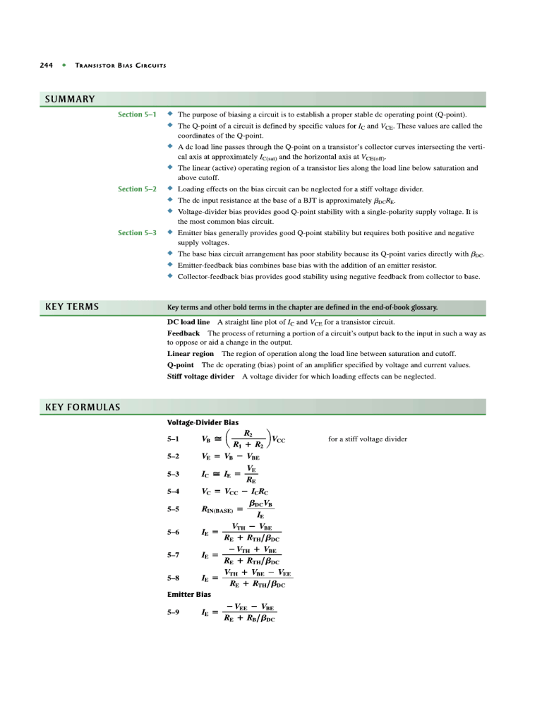
254 ♦ TRANSISTOR BIAS CIRCUITS ADVANCED PROBLEMS 49. Design a circuit using base bias that operates from a 15 V de voltage and draws a maximum current from the de source (lcqmax)) of 10 mA. The Q-point values are to be le = 5 mA and VCE = 5 V. The transistor is a 2N3904. Assume a midpoint value for /Joe. 50. Design a circuit using emitter bias that operates from de voltages of+ 12 V and -12 V. The maximum Ice is to be 20 mA and the Q-point is at 10 mA and 4 V. The transistor is a 2N3904. 51. Design a circuit using voltage-divider bias for the following specifications: Vee = 9 V, Icqmax) = 5 mA, le = 1.5 mA, and VCE = 3 V. The transistor is a 2N3904. 52. Design a collector-feedback circuit using a 2N2222A with Vee = 5V, le = 10 mA, and VCE = 1.5V. 53. Can you replace the 2N3904 in Figure 5--47 with a 2N2222A and maintain the same range of output voltage over a temperature range from 45°C to 55°C? 54. Refer to the datasheet graph in Figure 5-50 and the partial datasheet in Figure 5--49. Determine the minimum de current gain for a 2N2222A at -55°C, 25°C, and 175°C for VCE = 1 V. Ci ·c1 4.0 3.0 i:i 2.0 .g - _,_ ... 0.7 Ci J 0.3 � ,_ ,_ - ... 1.0 0.5 T1 = 175° C f- 0.2 0.5 _,_ ... - - 25° C ,_ i-- 1,_ I ... - - -- - - - - ---- -� �- -- .... ... - - -- - - - - - -... �- - -·- ... 55° c -- - - - I I I I Vrn = 1.0V- - - Vrn = lOV- � r-.... i::. ..... '- � "'- r-' � " - -- -.. '0 '" ' � ,� -� "� - 'I: '\ \ '\: 0.7 1.0 2.0 3.0 5.0 10 20 30 50 70 100 I'300 200 500 le, collector current (mA) _. FIGURE 5-50 55. A design change is required in the valve interface circuit of the temperature-control system shown in Figure 5-28. The new design will have a valve interface input resistance of 10 kll. Determine the effect this change has on the temperature-to-voltage conversion circuit. 56. Investigate the feasibility of redesigning the temperature-to-voltage conversion circuit in Figure 5-29 to operate from a de supply voltage of 5.1 V and produce the same range of output volt­ ages determined in the Device Application over the required thermistor temperature range from 60°C to 80°C. MULTISIM TROUBLESHOOTING PROBLEMS These file circuits are in the Troubleshooting Problems folder on the website. 57. Open file TPM05-57 and determine the fault. 58. Open file TPM05-58 and determine the fault. 59. Open file TPM05-59 and determine the fault. 60. Open file TPM05-60 and determine the fault. 61. Open file TPM05-61 and determine the fault. 62. Open file TPM05-62 and determine the fault.
