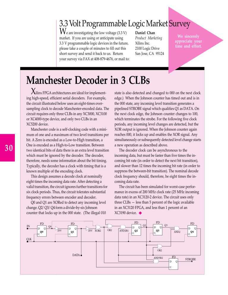
3.3 Volt Programmable Logic Market Survey We are investigating the low voltage (3.3 V) Daniel Chan We sincerely market. If you are using or anticipate using 3.3 V programmable logic devices in the future, please take a couple of minutes to fill out this short survey and send it back to us. Return your survey via FAX at 408-879-4676, or mail to: Product Marketing Xilinx Inc. 2100 Logic Drive San Jose, CA 95124 appreciate your time and effort. Manchester Decoder in 3 CLBs X 30 ilinx FPGA architectures are ideal for implementing high-speed, efficient serial decoders. For example, the circuit illustrated below uses an eight-times oversampling clock to decode Manchester-encoded data. The circuit requires only three CLBs in any XC3000, XC3100 or XC4000-type device, and only two CLBs in an XC5200 device. Manchester code is a self-clocking code with a minimum of one and a maximum of two level transitions per bit. A Zero is encoded as a Low-to-High transition, a One is encoded as a High-to-Low transition. Between two identical bits of data there is an extra level transition which must be ignored by the decoder. The decoder, therefore, needs some information about the bit timing. Typically, the decoder has a clock with timing that is a known multiple of the encoding clock. This design assumes a decode clock at nominally eight times the incoming data rate. After detecting a valid transition, the circuit ignores further transitions for six clock periods. Thus, the circuit tolerates substantial frequency errors between encoder and decoder. Q0 and Q1 are XORed to detect any incoming level change. Q2/Q3/Q4 form a divide-by-six Johnson counter that locks up in the 000 state. (The illegal 010 state is also detected and changed to 000 on the next clock edge.) When the Johnson counter has timed out and is in the 000 state, any incoming level transition generates a pipelined STROBE signal which qualifies Q1 as DATA. On the next clock edge, the Johnson counter changes to 100, which terminates the strobe. For the following five clock periods, any incoming level changes are detected, but the XOR output is ignored. When the Johnson counter again reaches 000, it locks up and enables the XOR signal. Any simultaneously or subsequently detected level change starts a new operation as described above. The decoder clock can be asynchronous to the incoming data, but must be faster than five times the incoming bit rate (in order to detect the next bit transition), and slower than 12 times the incoming bit rate (in order to suppress the between-bit transition). The nominal decode clock frequency should, therefore, be eight times the incoming data rate. The circuit has been simulated for worst-case performance in excess of 200 MHz clock rate (25 MHz incoming data rate) in an XC3120-2 device. The circuit uses only three CLBs — less than 5 percent of the logic available in an XC3120 FPGA, and less than 1 percent of an XC3190 device. ◆
