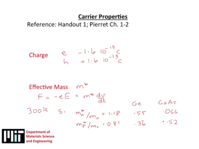
As far as gallium arsenide is concerned, the electrons have extremely low effective
mass. That means when we put an electric field on gallium arsenide, those electrons
will accelerate very fast so we can expect that gallium arsenide will have a very high
mobility. Those sorts of devices will work very quickly if we rely on electrons. On the
other hand if we rely on holes, we don't expect we will get a response as fast.
Effective masses determine the inertia with which your carriers, your electrons or
holes, move through the crystal if they happen to have energy of the conduction band
or valence band. In fact, the effective mass associated with the conduction band is
referred to as the effective mass of the electron. The effective mass of the valence
band is referred to as the effective mass of the holes. Usually, what you would find is
that conduction band is more curved than the valence band in real materials. So the
effective mass associated with the conduction band is lower than the effective mass
associated with the valence band. Generally, electrons are lighter than holes.
ntrins c Prope
'
= P - n..
...t
Ex
Do or
Acceptor
{)
I
------·--
Tl
------_)
Sn Sb Te
Pb Bi
Po
The very low concentration of carriers is an indication why material science was
actually an enabling technology for microelectronics because in order to observe
dopant effects and understand the behavior of these materials, we have to start
with very good quality, high purity materials and the purification methods that
were developed for silicon and other such materials.
For gallium arsenide, whether an atom is a donor or an acceptor that depends on which
side it is sitting. If silicon is sitting on the gallium side, then it would be a donor and
gallium is the acceptor. On the other hand if silicon is sitting on an arsenic side,
it would be an acceptor and arsenic is the donor. The dopant behavior in compound
semiconductors is rather more complicated.
Consider a group of N Si atoms
• Starting with N-isolated Si atoms, and bringing the atoms closer and closer
together, one finds the interatomic forces lead to a progressive spread in the
allowed energies
• The spread in energies give rise to closely spaced sets of allowed states known as
energy bands
• At the interatomic distance corresponding to the Si lattice spacing, the
distribution of allowed states consists of two bands separated by an intervening
energy gap
• The upper band of allowed state is called the conduction band (with 4N allowed
states); the lower band of allowed state, the valence band (with 4N allowed
states); and the intervening energy gap, the forbidden gap or band gap
• In filling the allowed energy band states, electrons tend to gravitate the lowest
possible energies
• Considering Pauli exclusion principle, 4N valence band states can accommodate 4N
valence electrons, so the valence band is almost completely filled with electrons
and the conduction band is all but devoid of electrons
• Indeed, the valence band is completed filled and the conduction band completely
empty at temperatures approaching 0K
• Unlike the valence electrons in the isolated-atom case, the band electrons in
crystalline silicon are not tied to or associated with any one particular atom
• The allowed electronic states are no longer atomic states but are associated with
the crystal as a whole.
The effective mass is different so the
slope of gc and gv is also different.
Since we only have finite number
of electrons(4N), the two curves
should eventually close up up on gc
and down on gv.
(gc,v)
Most of the actions happen
within this width of
approximately 3kT wide. The
Fermi function goes from 0 to
1 within this width and the
band gap is also contained in
there for electrons to exist in
the conduction band and holes
exist in the valence band.
semiconductor
= ni
(
)
for p
since Ev-Ec = -Eg
+
For
See next page
, Ei is
Later we will discuss conductivity depends not only on
the number of carriers, but also how mobile they are.
T
o a ri r
p ra r d p nd
,
n ity
We want to build
electronics in this
extrinsic region since
it is temperature
independent
-
f C
() ' . >
T
•
I'
)
sincen
n�i
=-
When we get up to very high doping levels, i.e. the order of 1020 or 1021, you're
not really talking about doping anymore. You're talking about alloying. You are at
the point where the doping atoms or acceptor atoms are no longer able to actually
dissolve in the silicon. So remember that whatever we're doping with needs to
dissolve into the lattice and give or accept electrons. If we can't have that, then
we're not going to get this electrical activity. That's why there's an upper bound
to the doping levels.
The lower bound to the doping levels is just that it's quite hard to control
purities on the order of parts per million or thereabouts. If you're making a
silicon ball or crystal, then you have a background doping level which is on the
order of 1014 or 1015 or thereabouts. You cannot really dope any less than that.
C r ri r dis ri u · o s
- Dens·ty of sta es g(E) shows how many elec ro s ca be
n rgy ng , d
p
e1 m fu , c ·0 ( ) elll s e p ob billi y hey are occ pi
Near he a d edge, he de si y of s a e i crease w
gr d o g·v o al n , mb r
T prod ct f( (E)d _ c
o e ec rans (o holes)
rm· I v
is w r f( ) - 0.5
A eq ilibri m, p = co s t = n?. nc eased te perature
raises np. Donor dopi g aises n a owers p, a d shi , s E 1 p.
Carri r co c ntration, nd h nc co d c ·vity, vari -s with T.
1
xt p: Carr er A
e
on


![Semiconductor Theory and LEDs []](http://s2.studylib.net/store/data/005344282_1-002e940341a06a118163153cc1e4e06f-300x300.png)