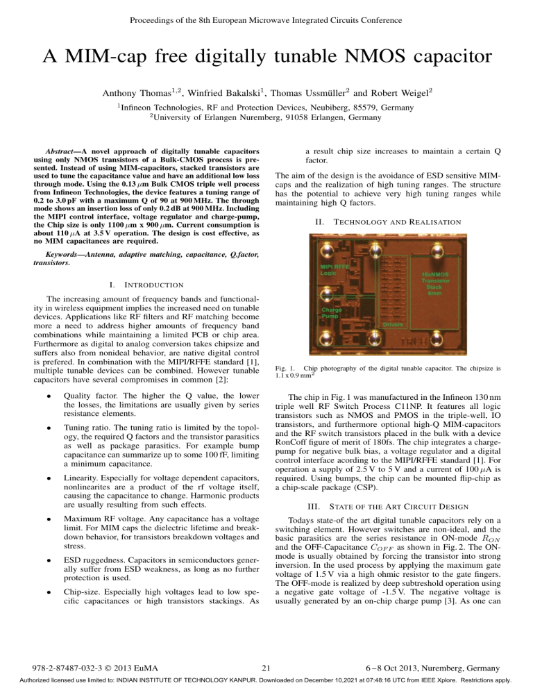
Proceedings of the 8th European Microwave Integrated Circuits Conference A MIM-cap free digitally tunable NMOS capacitor Anthony Thomas1,2 , Winfried Bakalski1 , Thomas Ussmüller2 and Robert Weigel2 1 Infineon Technologies, RF and Protection Devices, Neubiberg, 85579, Germany of Erlangen Nuremberg, 91058 Erlangen, Germany 2 University a result chip size increases to maintain a certain Q factor. Abstract—A novel approach of digitally tunable capacitors using only NMOS transistors of a Bulk-CMOS process is presented. Instead of using MIM-capacitors, stacked transistors are used to tune the capacitance value and have an additional low loss through mode. Using the 0.13 μm Bulk CMOS triple well process from Infineon Technologies, the device features a tuning range of 0.2 to 3.0 pF with a maximum Q of 90 at 900 MHz. The through mode shows an insertion loss of only 0.2 dB at 900 MHz. Including the MIPI control interface, voltage regulator and charge-pump, the Chip size is only 1100 μm x 900 μm. Current consumption is about 110 μA at 3.5 V operation. The design is cost effective, as no MIM capacitances are required. The aim of the design is the avoidance of ESD sensitive MIMcaps and the realization of high tuning ranges. The structure has the potential to achieve very high tuning ranges while maintaining high Q factors. II. T ECHNOLOGY AND R EALISATION Keywords—Antenna, adaptive matching, capacitance, Q.factor, transistors. I. I NTRODUCTION The increasing amount of frequency bands and functionality in wireless equipment implies the increased need on tunable devices. Applications like RF filters and RF matching become more a need to address higher amounts of frequency band combinations while maintaining a limited PCB or chip area. Furthermore as digital to analog conversion takes chipsize and suffers also from nonideal behavior, are native digital control is prefered. In combination with the MIPI/RFFE standard [1], multiple tunable devices can be combined. However tunable capacitors have several compromises in common [2]: • Quality factor. The higher the Q value, the lower the losses, the limitations are usually given by series resistance elements. • Tuning ratio. The tuning ratio is limited by the topology, the required Q factors and the transistor parasitics as well as package parasitics. For example bump capacitance can summarize up to some 100 fF, limiting a minimum capacitance. • Linearity. Especially for voltage dependent capacitors, nonlinearites are a product of the rf voltage itself, causing the capacitance to change. Harmonic products are usually resulting from such effects. • Maximum RF voltage. Any capacitance has a voltage limit. For MIM caps the dielectric lifetime and breakdown behavior, for transistors breakdown voltages and stress. • ESD ruggedness. Capacitors in semiconductors generally suffer from ESD weakness, as long as no further protection is used. • Chip-size. Especially high voltages lead to low specific capacitances or high transistors stackings. As 978-2-87487-032-3 © 2013 EuMA Fig. 1. Chip photography of the digital tunable capacitor. The chipsize is 1.1 x 0.9 mm2 The chip in Fig. 1 was manufactured in the Infineon 130 nm triple well RF Switch Process C11NP. It features all logic transistors such as NMOS and PMOS in the triple-well, IO transistors, and furthermore optional high-Q MIM-capacitors and the RF switch transistors placed in the bulk with a device RonCoff figure of merit of 180fs. The chip integrates a chargepump for negative bulk bias, a voltage regulator and a digital control interface acording to the MIPI/RFFE standard [1]. For operation a supply of 2.5 V to 5 V and a current of 100 μA is required. Using bumps, the chip can be mounted flip-chip as a chip-scale package (CSP). III. S TATE OF THE A RT C IRCUIT D ESIGN Todays state-of the art digital tunable capacitors rely on a switching element. However switches are non-ideal, and the basic parasitics are the series resistance in ON-mode RON and the OFF-Capacitance COF F as shown in Fig. 2. The ONmode is usually obtained by forcing the transistor into strong inversion. In the used process by applying the maximum gate voltage of 1.5 V via a high ohmic resistor to the gate fingers. The OFF-mode is realized by deep subtreshold operation using a negative gate voltage of -1.5 V. The negative voltage is usually generated by an on-chip charge pump [3]. As one can 21 6 -8 Oct 2013, Nuremberg, Germany Authorized licensed use limited to: INDIAN INSTITUTE OF TECHNOLOGY KANPUR. Downloaded on December 10,2021 at 07:48:16 UTC from IEEE Xplore. Restrictions apply. not be below 0.48 pF. As COF F scales with transistor width and this reciprocal to RON , one can see, that it ends up in a trade-off between tuning ratio and Qfactor. see, a level shifter is required for each switch to transfer the logic signal into a positive or negative gate voltage. NMOS IV. COFF Fig. 2. The NMOS transistor acting as a switch device. +/-V GATE Using this RF switch, todays digital tunable capacitors are designed using the series circuit of a cap and a switch device [4], weighted by N bits, with LSB (least significant bit) representing the smallest capacitance step and MSB (most significant bit) as the maximum switchable capacitance bit. Fig. 3 shows the usual circuit. COFF ... N COFF +/-V RON GATE GATE The main idea to achieve an alternative approach is the usage of the parasitic capacitance of a NMOS transistor itself. Hence, Using transistors of very high width automatically increases the parasitic capacitances, in switch processes dominated by CGS and CGD . Increasing the transistor width into the multi-mm region shifts the COF F into capacitance values of several pF. On the other hand, its high width leads to a very low RON . An additional effect of very high capacitance values is the limitation of RF voltage over the transistor, so that the capacitance automatically protects the transistor. Placing the high width transistors in series, a tunable capacitor can be realized just by the use of the parasitics. Fig. 4 shows the circuit diagram. NMOS +V T HE NMOS- BASED TUNABLE CAPACITANCE GATE GATE +/-V -V COFF MSB ... „N Bits“ Fig. 3. = Fig. 4. State-of-art digital tunable capacitor. ESD ruggedness is directly related to the MIM ESD performance. • The maximum allowed voltage of the capacitors. To achieve higher maximum voltages, several capacitors have to be switched in series. • The maximum RF transistor voltage. This usually limited by the ”OFF”-mode of the switches, when the impedance of the RF switch paths are far bigger than the capacitances, leading in a high RF voltage swing at the port of the stacked transistors. • The required Q-factor. For a high capacitance, a very low RON of the transistor is required. • The minimum capacitance Cmin which is resulting from the maximum capacitance switched in series to the overall COF F capacitance resulting from the transistors. Taking for simplicity a maximum capacitance of 10 pF and a COF F = 0.5 pF, the resulting Cmin can RON The NMOS based tunable capacitance. • The minimum capacitance and thus the tuning ratio is given by the stacking and not by the parasitic capacitance itself. • In case all transistors are switched to ON-mode, a very low loss bypass is found, due to the high transistor width and the low RON . Thus, the structure is inherently a Single-Pole-Single-Throw switch (SPST). • The Q factor is generally high due to its high transistor widthes and low RON . For low capacitances, the Q factor is high as well, as only parasitic capacitance is used. However it is in fact limited by the values of discharge resistors and gate resistors. • The structure gives more steps in the low capacitance range as for high capacitances. However this behavior can be changed by different transistor widths in the circuit. • The maximum voltage is not identical over all states, however the higher the COF F is selected, the lower the voltage stress will be. • The ESD ruggedness is only limited by the switch process technology used. The main trade-offs for this circuit are : • RON In comparison to Fig. 3, the structure has a different behavior: ... VGATE M stacked Devices ... ... Switch +/- VGATE M stacked Devices +/- M stacked Devices +/- VGATE RON W scales with C LSB ... ... ... High-Q MIM It is important to mention that this structure can only work, as long as the main capacitance contributor are the overlap 22 Authorized licensed use limited to: INDIAN INSTITUTE OF TECHNOLOGY KANPUR. Downloaded on December 10,2021 at 07:48:16 UTC from IEEE Xplore. Restrictions apply. Capacitance [pF] capacitances CGS and CGD is dominant. For this purpose, the substrate diodes have to be deactived. This is done by the usage of a negative substrate bias in combination with a low conductive substrate. In this case, the bulk bias generated by the same integrated charge-pump as required for the negative gate voltage to operate transistors in the deep subthreshold region. As this structure has N states, with N representing the amount of stacked transistors, a decoder to thermometer-code helps to reduce the amount of control bits. In the presented test-chip one RFFE register is mapped to a parallel to thermometercode decoder to address 16 transistors. In fact only 4 bits are required to adjust the required frequency. The state N-1 represents the ”all-ON” state, which is in series configuration a through mode. Finally all N transistors require its own level shifter to control each transistor. The main difference to a usual RF switch is, that the level shifter drives only one transistor. for less capacitances variation between states, it would be possible to stack double transistors for the same amount of control bits, thus, offering two times less capacitances but finer capacitances steps. 3.4 3.2 3 2.8 2.6 2.4 2.2 2 1.8 1.6 1.4 1.2 1 0.8 0.6 0.4 0.2 0 TRC1 0 1 2 3 4 5 6 7 8 9 10 11 12 13 14 State Fig. 6. Adjustable capacitance values vs. logic state. 100 90 Q at 900MHz Q at 1800MHz 80 V. M EASUREMENT R ESULTS 70 Q factor Fig. 5 shows the test board. The chip was measured in series configuration using a flip-chip package. All states were sweeped to obtain all capacitance values. Finally, capacitance values and Q factors extracted. 60 50 40 30 20 10 0 0 1 2 3 4 5 6 7 8 9 10 11 12 13 14 State Fig. 7. Fig. 5. Measured Q factor vs logic state. To evaluate the linearity of the device, the harmonics generation measurement setup in Fig. 8 is used. A constant wave signal is generated in pulse mode with 50 % duty cycle and 577 Hz pulse width and amplified using a power amplifier (PA). To ensure no damage or harmonics or other spurs due to output mismatch, an isolator is placed at the PA output. Also an additional low pass filter at input and high pass filter at output are placed respectively to filter out the potential 2nd and 3rd harmonics generated by the DUT from the input and isolate the fundamental input signal from the spectrum analyser to obtain the required dynamic range. As a capacitor can be used in different combinations, two configurations have to be tested. One would be the series configuration, here using the bypass mode and the other the shunt configuration, setting the device to minimum capacitance. In shunt configuration, usually the high RF voltage is seen by the device. Flip-chip mounted capacitance tuner used for the measurement. Fig. 6 shows the adjustable capacitances. In the given testchip, the capacitance can be tuned between 0.2 pF and 3 pF. By looking at the curve of capacitance versus steps, it appears that the curve follows as expected, the COF F of a single NMOS over the ratio of all OFF transistors. Thus, for double sized transistors, one could even reach higher capacitances. The first half states could be definitely useful for high frequencies due to their fine steps. This is an advantage of this topology compared with the capacitance bank in Fig. 3 which is limited by his overall COF F . The Fig. 9 and the Fig. 10 presents the 2nd and 3nd harmonic generation vs. input power of the test chip in ON-mode and OFF-mode respectively in parallel and series configuration at 824 MHz. The corresponding Q factor is shown in Fig. 7 for 900 MHz and 1.8 GHz. The Through mode related with the test chip shows an insertion loss of 0.2 dB at 900 MHz and 0.27 dB at 1.8 GHz. Addtionally, the MIM-cap free design provides excellent 23 Authorized licensed use limited to: INDIAN INSTITUTE OF TECHNOLOGY KANPUR. Downloaded on December 10,2021 at 07:48:16 UTC from IEEE Xplore. Restrictions apply. circuits are inherently digital devices, BST is by nature a varactor. Thinking of digital interfaces, varactors imply the need on Digital Analog Converters (DAC) and thus have all their drawbacks. MEMS are found in a lot of different configurations and types. To compare BST, typical MEMS and this approach some key figures are summarized in the Table. I. The major advantage of a CMOS capacitance bank is that the tuning range can easily be extended, and that a digital device as shown here is not impacted by temperature, analog control voltages and has no limitations in switching cylces. As well switching times are by far better than MEMS or BST. However, in terms of losses, MEMs present higher quality factor at 1 GHz, but suffer from all mechanic disadvantages such as limited switching cycles or microphony effects. BST varactors have always inherent linearity problems due to their varactor nature and feature a very low tuning range. On top BSTs can not be integrated today into silicon and require an external controller consuming 10 times more current than other solutions [7]. Regarding MEMS, a high voltage is required to commutate the switches and improve the switching time between maximum and minimum states [8]. Fig. 8. Harmonic measurement Setup of the DUT. 0 -10 H2 [dBm] state 0 parallel H3 [dBm] state 0 parallel Harmonic level [dBm] -20 -30 -40 -50 -60 -70 -80 TABLE I. -100 -110 C OMPARISON BETWEEN DIFFERENT TECHNOLOGIES OF TUNABLE CAPACITANCES -90 Type Current consumption Value (pF) Tuning Range Q factor(Max) @1 GHz Logic Control Switching time (μs) 20 22 24 26 28 30 32 34 36 38 Pin [dBm] 824MHz Fig. 9. 2nd and 3rd generated harmonics versus input power in parallel on OFF-mode position at 824 MHz. BST Varactor[5] ∼1 mA 0.3-1.2 4 90 External 70 VII. 0 -10 This Work 110 μA 0.2-3 15 85 integrated <2 C ONCLUSION A novel method of tunable capacitance is presented on this paper. It shows a concept based on stacked transistors using drain source capacitance in order to generate a tunable capacitor. The capacitance can be changed from 0.2 pF until 3.0 pF with a low loss bypass mode of 0.2 dB at 900 MHz. and 0.27 dB at 1800 MHz. The structure has a Q factor of up to 90 at 900 MHz, while not requiring any high Q MIM capacitance. H2 [dBm] state 15 series H3 [dBm] state 15 series -20 Harmonic level [dBm] MEMS [6] ∼100 μA 0.13-1.27 10 160 integrated >10 [8] -30 -40 -50 -60 -70 R EFERENCES -80 [1] -90 [2] -100 -110 [3] 20 22 24 26 28 30 32 34 36 38 Pin [dBm] 824MHz [4] Fig. 10. 2nd and 3rd generated harmonics versus input power in series on ON-mode position at 824 MHz. [5] [6] ESD behavior. This is proved using Transmission Line Pulse (TLP) measurements. The structure can handle more than 2 kV of ESD discharge according to the human body model. VI. [7] [8] T ECHNOLOGY COMPARISONS Recent Works in specialized technologies like Barium Strontium Titanat (BST) [5] and MEMS [6] show interesting results as variable capacitors. Whereas CMOS switch based MIPI Alliance, “RF Front-End Specifications,” http://www.mipi.org/specifications/rf-front-end. R. Novak, “IWPC Tunable Components and Platform Architectures for Smartphone,” Presentation at IWPC 2012, November 2012. F. Pan and T. Samaddar, Charge Pump Circuit Design. New York, USA: McGraw-Hill, 2006. R. Whatley, T. Ranta, and D. Kelly, “CMOS Based Tunable Matching Networks for Cellular Handset Applications,” Proceedings of the Internation Microwave Symposium 2011, 2011. “BST passive tunable integrated circuit,” ON semiconductors, http://www.onsemi.com/pub link/Collateral/TCP-3012H-D.PDF. D. DeReus et al., “Tunable capacitor series/shunt design for integrated tunable wireless front end applications,” MEMS, 2011 IEEE 24th International Conference, pp. 805–808, Jan. 2011. “Passive tunable integrated circuit control IC,” ON semiconductors, http://www.onsemi.com/pub link/Collateral/TCC-103-D.PDF. A. Tazzoli et al., “Electrostatic discharge and cycling effects on ohmic and capacitive rf-mems switches,” IEEE Transactions on Device and Materials Reliabiliy, pp. 429–437, 2007. 24 Authorized licensed use limited to: INDIAN INSTITUTE OF TECHNOLOGY KANPUR. Downloaded on December 10,2021 at 07:48:16 UTC from IEEE Xplore. Restrictions apply.


