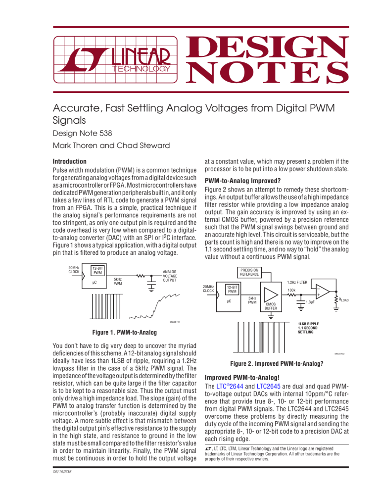
Accurate, Fast Settling Analog Voltages from Digital PWM Signals Design Note 538 Mark Thoren and Chad Steward Introduction Pulse width modulation (PWM) is a common technique for generating analog voltages from a digital device such as a microcontroller or FPGA. Most microcontrollers have dedicated PWM generation peripherals built in, and it only takes a few lines of RTL code to generate a PWM signal from an FPGA. This is a simple, practical technique if the analog signal’s performance requirements are not too stringent, as only one output pin is required and the code overhead is very low when compared to a digitalto-analog converter (DAC) with an SPI or I2C interface. Figure 1 shows a typical application, with a digital output pin that is filtered to produce an analog voltage. 20MHz CLOCK 12-BIT PWM µC 5kHz PWM at a constant value, which may present a problem if the processor is to be put into a low power shutdown state. PWM-to-Analog Improved? Figure 2 shows an attempt to remedy these shortcomings. An output buffer allows the use of a high impedance filter resistor while providing a low impedance analog output. The gain accuracy is improved by using an external CMOS buffer, powered by a precision reference such that the PWM signal swings between ground and an accurate high level. This circuit is serviceable, but the parts count is high and there is no way to improve on the 1.1 second settling time, and no way to “hold” the analog value without a continuous PWM signal. PRECISION REFERENCE ANALOG VOLTAGE OUTPUT 20MHz CLOCK 1.2Hz FILTER 12-BIT PWM µC DN538 F01 Figure 1. PWM-to-Analog You don’t have to dig very deep to uncover the myriad deficiencies of this scheme. A 12-bit analog signal should ideally have less than 1LSB of ripple, requiring a 1.2Hz lowpass filter in the case of a 5kHz PWM signal. The impedance of the voltage output is determined by the filter resistor, which can be quite large if the filter capacitor is to be kept to a reasonable size. Thus the output must only drive a high impedance load. The slope (gain) of the PWM to analog transfer function is determined by the microcontroller’s (probably inaccurate) digital supply voltage. A more subtle effect is that mismatch between the digital output pin’s effective resistance to the supply in the high state, and resistance to ground in the low state must be small compared to the filter resistor’s value in order to maintain linearity. Finally, the PWM signal must be continuous in order to hold the output voltage 05/15/538 – + 100k 5kHz PWM CMOS BUFFER 1.3µF RLOAD 1LSB RIPPLE 1.1 SECOND SETTLING DN538 F02 Figure 2. Improved PWM-to-Analog? Improved PWM-to-Analog! The LTC ®2644 and LTC2645 are dual and quad PWMto-voltage output DACs with internal 10ppm/°C reference that provide true 8-, 10- or 12-bit performance from digital PWM signals. The LTC2644 and LTC2645 overcome these problems by directly measuring the duty cycle of the incoming PWM signal and sending the appropriate 8-, 10- or 12-bit code to a precision DAC at each rising edge. L, LT, LTC, LTM, Linear Technology and the Linear logo are registered trademarks of Linear Technology Corporation. All other trademarks are the property of their respective owners. An internal 1.25V reference sets the full-scale output to 2.5V, and an external reference can be used if a different full-scale output is required. A separate IOVCC pin sets the digital input level, allowing a direct connection to 1.8V FPGAs, 5V microcontrollers, or any voltage between. DC accuracy specifications are excellent, with 5mV offset, 0.8% maximum gain error, and 2.5LSB (12-bit) maximum INL. Output settling time is 8µs from the rising edge of the PWM input to within 0.024% of the final value (1LSB at 12 bits). The PWM frequency range is 30Hz to 6.25kHz for 12-bit versions. Versatile Output Modes Figure 4 shows a typical supply trim/margining application that takes advantage of yet another unique feature of the LTC2644. Tying IDLSEL high selects “sample/ hold” operation; outputs are high impedance at start-up (no margining), a continuous high level on the input causes the output to hold its value indefinitely, and a continuous low level puts the output into a high impedance state. Thus the supply can be trimmed once at power-up with a PWM burst followed by a high level. Pulling the PWM signal low allows the circuit to cleanly exit a margining operation. Tying IDLSEL to GND selects “transparent mode,” in which a continuous high level on the input sets the output to full-scale, and a continuous low level sets the output to zero-scale. Conclusion Don’t despair if you come face to face with the limitations of typical PWM to analog techniques. The LTC2645 makes it possible to produce accurate, fast-settling analog signals from pulse-width modulated digital outputs while maintaining low parts count and code simplicity. PWM INPUTS INA VOUTA INB VOUTB INC VOUTC IND 1.7V TO 5.5V INA 2V/DIV VOUTD LTC2645 IOVCC REF PD 0.1µF BUFFERED VOLTAGE OUTPUTS INPUT: 1V TO 5.5V OUTPUT: 1.25V 2.7V TO 5.5V VCC GND IDLSEL 0.1µF REFSEL 0.1µF VOUTA 500mV/DIV GND DN538 F03b 20µs/DIV DN538 F03a Figure 3. 4-Channel PWM-to-Analog 5V C3 0.1µF C4 0.1µF 0.1µF 4.7µF 2.2k IOVCC VCC IDLSEL REFSEL PD INA INB 0.1µF DAC A VOUTA 10k ILM 143k DAC B VOUTB PGOOD INTVCC LTC3850EUF 10k 0.1µF PWM TO BINARY VIN RJK0305DPB TG1 BOOST1 FREQ 0.1µF 2.2µH 0.008k SW1 VOUTB = Hi-Z 1nF CMDSH-3 100k REF LTC2644-12 PWM TO BINARY VIN 6.5V TO 14V 3.32k VOUT 3.3V ±10% RJK0301DPB BG1 PGND GND FOR NO MARGINING, KEEP INA LOW. (VOUTA = Hi-Z) TO MARGIN 10% HIGH, SET INA DUTY CYCLE TO 1/4096. (VOUTA = 0V) TO MARGIN 10% LOW, SET INA DUTY CYCLE TO 2621/4096. (VOUTA = 1.6V) 1nF 10k 10k SENSE1+ ITH1 500kHz 100pF MODE/PLLIN RUN1 1nF SENSE1– TKSS1 10nF 10k VFB1 SGND 15pF 63.4k 20k DN538 F04 Figure 4. Margining Application Data Sheet Download www.linear.com/LTC2644 Linear Technology Corporation For applications help, call (408) 432-1900, Ext. 3799/3718 dn538f LT/AP 0515 111K • PRINTED IN THE USA 1630 McCarthy Blvd., Milpitas, CA 95035-7417 (408) 432-1900 ● FAX: (408) 434-0507 ● www.linear.com LINEAR TECHNOLOGY CORPORATION 2015
