JFET & MOSFET Worksheet: Characteristics, Parameters, Biasing
advertisement
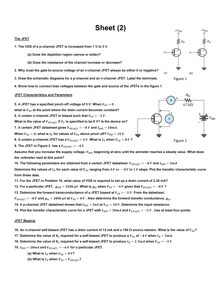
Sheet (2) The JFET 1. The VGS of a p-channel JFET is increased from 1 V to 3 V. (a) Does the depletion region narrow or widen? (b) Does the resistance of the channel increase or decrease? 2. Why must the gate-to-source voltage of an n-channel JFET always be either 0 or negative? 3. Draw the schematic diagrams for a p-channel and an n-channel JFET. Label the terminals. Figure 1 4. Show how to connect bias voltages between the gate and source of the JFETs in the figure 1 JFET Characteristics and Parameters 5. A JFET has a specified pinch-off voltage of 5 V. When ࡳࡿ , what is ࡰࡿ at the point where the drain current becomes constant? 6. A certain n-channel JFET is biased such that ࡳࡿ . What is the value of ࡳࡿሺࢌࢌሻ if ࡼ is specified to be 6 V? Is the device on? 7. A certain JFET datasheet gives ࡳࡿሺࢌࢌሻ and ࡰࡿࡿ When ࡳࡿ , what is ࡰ for values of ࡰࡿ above pinch off? ࡰࡰ 8. A certain p-channel JFET has a ࡳࡿሺࢌࢌሻ . . . What is ࡰ when ࡳࡿ ? Figure 2 9. The JFET in Figure 2 has a ࡳࡿሺࢌࢌሻ Assume that you increase the supply voltage, ࡰࡰ , beginning at zero until the ammeter reaches a steady value. What does the voltmeter read at this point? 10. The following parameters are obtained from a certain JFET datasheet: ࡳࡿሺࢌࢌሻ and ࡰࡿࡿ Determine the values of ࡰ for each value of ࡳࡿ ranging from in steps. Plot the transfer characteristic curve from these data. 11. For the JFET in Problem 10, what value of VGS is required to set up a drain current of 2.25 mA? 12. For a particular JFET, . What is when ࡳࡿ given that ࡳࡿሺࢌࢌሻ ? 13. Determine the forward transconductance of a JFET biased at ࡳࡿ . From the datasheet, ࡳࡿሺࢌࢌሻ and at ࡳࡿ . Also determine the forward transfer conductance, ࢌ࢙ 14. A p-channel JFET datasheet shows that ࡳࡿࡿ at ࡳࡿ . Determine the input resistance. 15. Plot the transfer characteristic curve for a JFET with ࡰࡿࡿ and ࡳࡿሺࢌࢌሻ . Use at least four points. JFET Biasing 16. An n-channel self-biased JFET has a drain current of 12 mA and a 100 Ω source resistor. What is the value of ࡳࡿ ? 17. Determine the value of ࡿ required for a self-biased JFET to produce a ࡳࡿ of when ࡰ 18. Determine the value of ࡿ required for a self-biased JFET to produce ࡰ . 19. ࡰࡿࡿ and ࡳࡿሺࢌࢌሻ for a particular JFET. (a) What is ࡰ when ࡳࡿ ? (b) What is ࡰ when ࡳࡿ ࡳࡿሺࢌࢌሻ ? when ࡳࡿ . (c) If ࡳࡿ is increased from , does ࡰ increase or decrease? 20. For each circuit in Figure 3, determine ࡰࡿ and ࡳࡿ . Figure 3 21. Using the curve in Figure 4, determine the value of ࡿ required for a 9.5 mA drain current. 22. Set up a midpoint bias for a JFET with ࡰࡿࡿ and ࡳࡿሺࢌࢌሻ . Use a 24 V dc source as the supply voltage. Show the circuit and resistor values. Indicate the values of ࡰ , ࡳࡿ , and ࡰࡿ. 23. Determine the total input resistance in Figure 5. ࡳࡿࡿ at ࡳࡿ . 24. Graphically determine the Q-point for the circuit in Figure 6(a) using the transfer characteristic curve in Figure 6(b). Figure 4 Figure 5 Figure 6 25. Find the Q-point for the p-channel JFET circuit in Figure 7. Figure 7 26. Given that the drain-to-ground voltage in Figure 8 is 5 V, determine the Q-point of the circuit. 27. Find the Q-point values for the JFET with voltage-divider bias in Figure 9. Figure 8 Figure 9 The MOSFET 28. Draw the schematic symbols for n-channel and p-channel E-MOSFETs and D-MOSFETs. Label the terminals. 29. In what mode is an n-channel D-MOSFET with a positive VGS operating? 30. Describe the basic difference between an E-MOSFET and a D-MOSFET. 31. Explain why both types of MOSFETs have an extremely high input resistance at the gate. MOSFET Characteristics and Parameters 32. The datasheet for a certain D-MOSFET gives ࡳࡿሺࢌࢌሻ and ࡰࡿࡿ (a) Is this device p channel or n channel? (b) Determine ࡰ for values of ࡳࡿ ranging from in increments of . (c) Plot the transfer characteristic curve using the data from part (b). 33. Determine ࡰࡿࡿ, given ࡰ , ࡳࡿ , and ࡳࡿሺࢌࢌሻ 34. The datasheet for an E-MOSFET reveals that ࡰሺሻ at ࡳࡿ and ࡳࡿሺ࢚ࢎሻ Find ࡰ when ࡳࡿ . MOSFET Characteristics and Parameters 35. Determine in which mode (depletion, enhancement or neither) each D-MOSFET in Figure 10 is biased. Figure 10 36. Each E-MOSFET in Figure 11 has a ࡳࡿሺ࢚ࢎሻ of depending on whether it is an n-channel or a p-channel device. Determine whether each MOSFET is on or off. Figure 11 37. Determine ࡰࡿ for each circuit in Figure 12. ࡰࡿࡿ . Figure 12 38. Find ࡳࡿ and ࡰࡿ for the E-MOSFETs in Figure 13. Datasheet information is listed with each circuit. Figure 13 39. Based on the ࡳࡿ measurements, determine the drain current and drain-to-source voltage for each circuit in Figure 14 Figure 14 40. Determine the actual gate-to-source voltage in Figure 15 by taking into account the gate leakage current, ࡳࡿࡿ . Assume that ࡳࡿࡿ is 50 pA and ࡰ is 1 mA under the existing bias conditions. Figure 15 Answer
