International Journal of Trend in Scientific Research and Development (IJTSRD)
Volume 4 Issue 5, July-August 2020 Available Online: www.ijtsrd.com e-ISSN: 2456 – 6470
Design and Implementation of Low Power Adiabatic
System for Power Recycling in Frequency Divider
K. Mahalakshmi1, S. Jabeentaj1, V. Kaviyamalai1, Mr. R. Thirumurugan2
1Student, 2Assistant
Professor,
of Electronics and Communication Engineering,
1,2S. A. Engineering College, Chennai, Tamil Nadu, India
1,2Department
ABSTRACT
Frequency divider to generate a frequency that is a multiple of a reference
frequency. The latch based frequency divider are cascaded the two static
differential sense amplifier pulsed latch (SSA SPL) with body biasing
techniques. The operation of this type divider is to reduce power, delay and
transistor size. The Adiabatic techniques dramatically reduce power
consumption. This paper presents (ECRL) Efficient Charge Recovery Logic
latch based frequency divider, which provides a contentment achievement.
The architecture is combined two latches with feedback. Thus, frequency
division is done. The circuit designed and simulation can be done in TANNER
EDA.
How to cite this paper: K. Mahalakshmi |
S. Jabeentaj | V. Kaviyamalai | Mr. R.
Thirumurugan
"Design
and
Implementation of Low Power Adiabatic
System for Power Recycling in Frequency
Divider" Published in
International Journal
of Trend in Scientific
Research
and
Development (ijtsrd),
ISSN:
2456-6470,
Volume-4 | Issue-5,
IJTSRD32953
August 2020, pp.838842,
URL:
www.ijtsrd.com/papers/ijtsrd32953.pdf
KEYWORDS: Low power, adiabatic, ECRL, frequency divider, SSASPLlatch, body
biasing technique
Copyright © 2020 by author(s) and
International Journal of Trend in Scientific
Research and Development Journal. This
is an Open Access article distributed
under the terms of
the
Creative
Commons Attribution
License
(CC
BY
4.0)
(http://creativecommons.org/licenses/by
/4.0)
I.
INTRODUCTION
Due to the reducing size of circuit in today’s generation of
vlsi technology. Storage elements will be classified into
latches and flip-flops. Latch is a device with two stable
states: low-output and high-output. A latch has a feedback
path, so information can be hold on by the device. Therefore
latches are called volatile memory devices, and stores only
one bit of data for as long as the device is powered. The
name itself suggests, latches are used to "latch onto"
information and hold in place.
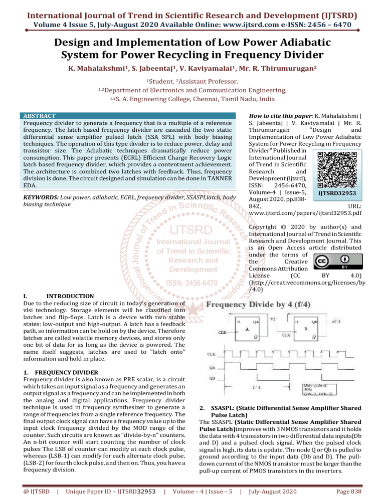
1. FREQUENCY DIVIDER
Frequency divider is also known as PRE scalar, is a circuit
which takes an input signal as a frequency and generates an
output signal as a frequency and can be implemented in both
the analog and digital applications. Frequency divider
technique is used in frequency synthesizer to generate a
range of frequencies from a single reference frequency. The
final output clock signal can have a frequency value up to the
input clock frequency divided by the MOD range of the
counter. Such circuits are known as “divide-by-n” counters.
An n-bit counter will start counting the number of clock
pulses The LSB of counter can modify at each clock pulse,
whereas (LSB-1) can modify for each alternate clock pulse,
(LSB-2) for fourth clock pulse, and then on. Thus, you have a
frequency division.
@ IJTSRD
|
Unique Paper ID – IJTSRD32953
|
2. SSASPL: (Static Differential Sense Amplifier Shared
Pulse Latch)
The SSASPL (Static Differential Sense Amplifier Shared
Pulse Latch)improves with 3 NMOS transistors and it holds
the data with 4 transistors in two differential data inputs(Db
and D) and a pulsed clock signal. When the pulsed clock
signal is high, its data is update. The node Q or Qb is pulled to
ground according to the input data (Db and D). The pulldown current of the NMOS transistor must be larger than the
pull-up current of PMOS transistors in the inverters.
Volume – 4 | Issue – 5
|
July-August 2020
Page 838
International Journal of Trend in Scientific Research and Development (IJTSRD) @ www.ijtsrd.com eISSN: 2456-6470
The number of transistors in SSASPL is less when compared
to flip-flop i.e., latch consists of 7 transistors where as flipflop consists of 16 transistors. The three NMOS transistors
are used to update the data and remaining transistors are
used for the operation.
Fig 3.2 Pulse clock generator waveform
VARIABLE BODY BIASING TECHNIQUE IMPLEMENTED IN
PULSE CLOCK GENERATOR MODULES
Fig: 2.1 SSASPL latch circuit
SSASPL latch truth table
3. OPERATIONINVOLVED IN THE BODY BIASING
Due to the reducing size of circuit in today’s generation of
vlsi technology. Storage elements will be classified into
latches and flip-flops. Latch is a device with two stable
states: low-output and high-output. A latch has a feedback
path, so information can be hold on by the device. Therefore
latches are called volatile memory devices, and stores only
one bit of data for as long as the device is powered. The
name itself suggests, latches are used to "latch onto"
information and hold in place.
Fig 3.3 AND gate circuit with biasing followed by truth
table and waveform
The above circuit shows the AND gate which is implemented
with body biasing technique to minimize the leakage power
which results in the low power consumption.
Fig 3.1 Basic body biasing
A body bias technique is proposed for leakage minimization
in frequency divider. The biasing technique is used in delay,
AND gate, NOT gate, buffer circuits in the pulse clock
generator as shown in the figure. Biasing reduces the leakage
power .It reduces the power consumption and increases the
performance of the circuit.
Fig 3.4 NOT gate circuit with biasing followed by truth
table and waveform
The above circuit shows the NOT gate which is implemented
with body biasing technique to minimize the leakage power
which results in the low power consumption.
Fig 3.2 Pulse generator circuit
@ IJTSRD
|
Unique Paper ID – IJTSRD32953
|
Volume – 4 | Issue – 5
|
July-August 2020
Page 839
International Journal of Trend in Scientific Research and Development (IJTSRD) @ www.ijtsrd.com eISSN: 2456-6470
III.
SIMULATION RESULTS
Fig 6.1 Schematic of AND gate circuit
The above ftorsigure shows the schematic of AND gate
circuit without biasing which is implemented with two
transis.
Fig 3.5 Delay circuit with biasing followed by
waveform
The above circuit shows the Delay circuit which is
implemented with body biasing technique to minimize the
leakage power which results in the low power consumption.
II.
Fig 6.2Simulation result of AND gate
The above figure shows the schematic of AND gate output.
PROPOSED SYSTEM
Fig 6.3 Schematic of NOT gate circuit
Fig 4 Circuit of frequency divider using SSASPL Latch
The above figure shows the schematic of NOT gate circuit
without biasing which is implemented with two transistors
Flip-flop operation is based on the clock signal which is the
main power consuming network in freqency divider. For
Frequency Division or as a “divide-by-2” counter. Here the
inverted output terminal Q (NOT-Q) is connected directly
back to the Data input terminal D giving the device
“feedback”
POWER CONSUMPTION TABLE
Power
Pc with body
Circuit
consumption(Pc)
biasing
-007
AND gate
3.084146e W
2.523468e-007W
Buffer
1.178229e-006W
8.453198e-007W
Delay
1.028487e-004W
4.285585e-005W
-009
NOT gate
2.726574e W
1.9083478e-11W
CLK-pulse
1.938271e-004W
9.917125e-005W
generator
Frequency
1.016487e-001W
4.841338e-003W
divider
Table.5.1. comparison table for power consumption
with biasing and without biasing
@ IJTSRD
|
Unique Paper ID – IJTSRD32953
|
Fig 6.4Simulation result of NOT gate circuit
.
The above figure shows the schematic of NOT gate output.
Fig 6.5 Schematic of Delay circuit
Volume – 4 | Issue – 5
|
July-August 2020
Page 840
International Journal of Trend in Scientific Research and Development (IJTSRD) @ www.ijtsrd.com eISSN: 2456-6470
The above figure shows the schematic of Delay circuit with
biasing which is implemented with 8-transistors to reduce
the leakage.
Fig 6.6 Simulation result of Delay circuit
The above figure shows the schematic of pulse clock
generator which consisting of delay, AND gate, NOT gate
and it produces 5-clock pulses.
Fig 6.10 Simulation result of Pulse clock generator
The above figure shows the schematic of Delay output with
biasing.
The above figure shows the schematic of Pulse clock
generator output with biasing.
Fig 6.11 Schematic of frequency divider design
Fig6.7 Schematic of SSASPL circuit
The above figure shows the schematic of Static Differential
Sense Amplifier Shared Pulsed Latch circuit which consists
of 7-transistors.
The above figure shows the schematic of frequency divider
circuit with pulsed latches.
Fig 6.12Simulation result of frequency divider design
The above figure shows the schematic of shift register circuit
with pulsed latches output with biasing.
Fig 6.8Schematic result of SSASPL circuit
The above figure shows the schematic of SSASPL output with
biasing.
Fig 6.13 Schematic of frequency divider design with
biasing
Fig 6.9 Schematic of Pulse clock generator
@ IJTSRD
|
Unique Paper ID – IJTSRD32953
|
The above figure shows the schematic of frequency divider
circuit with pulsed latches.
Volume – 4 | Issue – 5
|
July-August 2020
Page 841
International Journal of Trend in Scientific Research and Development (IJTSRD) @ www.ijtsrd.com eISSN: 2456-6470
which are additional. A frequency divider was fabricated
using a 0.45 CMOS process width. Its core area is. It
consumes 1.8mW at a 10 MHz clock frequency. The
proposed frequency divider saves 50% area and 30% to
50% power compared to the flip flop using frequency
divider.
Fig 6.14 Simulation result of frequency divider design
with biasing
The above figure shows the schematic of shift register circuit
with pulsed latches output with biasing
Fig 6.13 power consumption of frequency divider with
biasing
Fig 6.14 power consumption of frequency divider
without biasing
Circuit Width Length
AND
Buffer 2.50μ
0.25μ
Delay
NOT
Latch
1μ
0.18μ
Table 6.1 Length and width
|
Unique Paper ID – IJTSRD32953
[2] S.-H. W. Chiang and S. Kleinfelder, “Scaling and design
of a 16-megapixel CMOS image sensor for electron
microscopy,” in Proc. IEEENucl. Sci. Symp. Conf. Record
(NSS/MIC), 2009, pp. 1249–1256.
[3] M. Hatamian et al., “Design considerations for gigabit
ethernet 1000 base-T twisted pair transceivers,” Proc.
IEEE Custom Integr. CircuitsConf., pp. 335–342, 1998.
[4] S. Heo, R. Krashinsky, and K. Asanovic, “Activitysensitive flip-flop and latch selection for reduced
energy,” IEEE Trans. Very Large ScaleIntegr. (VLSI)
Syst., vol. 15, no. 9, pp. 1060–1064, Sep. 2007.
[5] H.-S. Kim, J.-H. Yang, S.-H. Park, S.-T. Ryu, and G.-H. Cho,
“A 10-bit column-driver IC with parasitic-insensitive
iterative charge-sharing based capacitor-string
interpolation for mobile active-matrix LCDs,” IEEE J.
Solid-State Circuits, vol. 49, no. 3, pp. 766–782, Mar.
2014.
[6] S. Naffziger and G. Hammond, “The implementation of
the next generation 64 b itanium microprocessor,” in
IEEE Int. Solid-State CircuitsConf. (ISSCC) Dig. Tech.
Papers, Feb. 2002, pp. 276–504.
IV.
CONCLUSION
The Frequency divider reduces power consumption and area
by replacing flip-flops with pulsed latches. The timing
problem between pulsed latches is solved by placing delay
circuits in between clock pulse signals. The small number of
the pulsed clock signals is used by categorizing the latches to
several frequency and using temporary storage latches
@ IJTSRD
REFERENCE:
[1] E. Consoli, M. Alioto, G. Palumbo, and J. Rabaey,
“Conditional push-pull pulsed latch with 726 fJops
energy delay product in 65 nm CMOS,” in IEEE Int.
Solid-State Circuits Conf. (ISSCC) Dig. Tech. Papers, Feb.
2012, pp. 482–483.
|
[7] H. Partovi et al., “Flow-through latch and edgetriggered flip-flop hybrid elements,” IEEE Int. SolidState Circuits Conf. (ISSCC) Dig. Tech.Papers, pp. 138–
139, Feb. 1996.
[8] P. Reyes, P. Reviriego, J. A. Maestro, and O. Ruano, “New
protection techniques against SEUs for moving average
filters in a radiation environment,” IEEE Trans. Nucl.
Sci., vol. 54, no. 4, pp. 957–964, Aug. 2007.
Volume – 4 | Issue – 5
|
July-August 2020
Page 842
