PBL3717A
STEPPER MOTOR DRIVER
.
..
.
..
.
.
FULL STEP - HALF STEP - QUARTER STEP
OPERATING MODE
BIPOLAR OUTPUT CURRENT UP TO 1 A
FROM 10 V UP TO 46 V MOTOR SUPPLY
VOLTAGE
LOW SATURATION VOLTAGE WITH INTEGRATED BOOTSTRAP
BUILT IN FAST PROTECTION DIODES
EXTERNALLY
SELECTABLE CURRENT
LEVEL
OUTPUT CURRENT LEVEL DIGITALLY OR
ANALOGUE CONTROLLED
THERMAL PROTECTION WITH SOFT INTERVENTION
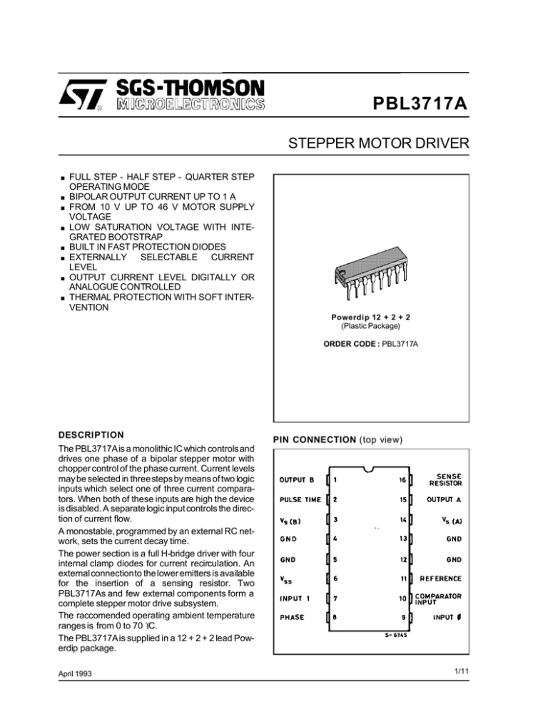
Powerdip 12 + 2 + 2
(Plastic Package)
ORDER CODE : PBL3717A
DESCRIPTION
PIN CONNECTION (top view)
The PBL3717Ais a monolithic IC which controls and
drives one phase of a bipolar stepper motor with
chopper control of the phase current. Current levels
may be selected in threesteps by means of two logic
inputs which select one of three current comparators. When both of these inputs are high the device
is disabled. A separate logic input controls the direction of current flow.
A monostable, programmed by an external RC network, sets the current decay time.
The power section is a full H-bridge driver with four
internal clamp diodes for current recirculation. An
externalconnectionto the lower emitters is available
for the insertion of a sensing resistor. Two
PBL3717As and few external components form a
complete stepper motor drive subsystem.
The raccomended operating ambient temperature
ranges is from 0 to 70 °C.
The PBL3717Ais supplied in a 12 + 2 + 2 lead Powerdip package.
April 1993
1/11
PBL3717A
PIN FUNCTIONS
N°
Name
Function
1
UTPUT B
Output Connection (with pin 15). The output stage is a ”H” bridge formed by four
transistors and four diodes suitable for switching applications.
2
PULSE TIME
A parallel RC network connected to this pin sets the OFF time of the lower power
transistors. The pulse generator is a monostable triggered by the rising edge of
the output of the comparators (toff = 0.69 RT CT).
3
SUPPLY VOLTAGE B
4
GROUND
Supply Voltage Input for Half Output Stage
See also pin 14.
Ground Connection. With pins 5, 12 and 13 also conducts heat from die to
printed circuit copper.
5
GROUND
6
LOGIC SUPPLY
See pin 4.
7
INPUT 1
This pin and pin 9 (INPUT 0) are logic inputs which select the outputs of the
three comparators to set the current level. Current also depends on the sensing
resistor and reference voltage. See truth table.
8
PHASE
This TTL-compatible logic input sets the direction of current flow through the
load. A high level causes current to flow from OUTPUT A (source) to OUTPUT
B (sink). A schmitt trigger on this input provides good noise immunity and a delay
circuit prevents output stage short circuits during switching.
9
INPUT 0
See INPUT 1 (pin 7) .
10
COMPARATOR
INPUT
Input connected to the three comparators. The voltage across the sense resistor
is feedback to this input through the low pass filter RC CC. The lower power
transistor are disabled when the sense voltage exceeds the reference voltage of
the selected comparator. When this occurs the current decays for a time set by
RT CT, toff = 0.69 RT C T.
11
REFERENCE
A voltage applied to this pin sets the reference voltage of the three comparators,
this determining the output current (also thus depending on R s and the two inputs
INPUT 0 and INPUT 1).
12
GROUND
Supply Voltage Input for Logic Circuitry
See pin 4.
13
GROUND
14
SUPPLY VOLTAGE A
See pin 4.
15
OUTPUT A
16
SENSE RESISTOR
Supply Voltage Input for Half Output Stage. See also pin 13.
See pin 1.
Connection to Lower Emitters of Output Stage for Insertion of Current Sense
Resistor
TRUTH TABLE
Inpu t 0 (pin 9)
Input 1 (pin 7)
H
L
H
L
H
H
L
L
2/11
No Current
Low Current
Medium Current
High Current
PBL3717A
BLOCK DIAGRAM
ABSOLUTE MAXIMUM RATINGS
Symbol
Parameter
Value
Unit
Vs
Power Supply Voltage
50
V
Vss
Logic Supply Voltage
7
V
Vi
Logic Input Voltage
6
V
Vc
Comparator Input
Vr
Reference Input Voltage
15
V
Io
Output Current (DC operation)
1.2
A
– 55 to + 150
°C
150
°C
Tstg
Tj
Vss
Storage Temperature
Operating Junction Temperature
THERMAL DATA
Symbol
Value
Unit
Rth j-case
Thermal Resistance Junction-pins
Parameter
11
°C/W
Rth j-amb
Thermal Resistance Junction-ambient*
40
°C/W
* Soldered on a 35µ thick 20 cm2 P.C. board copper area.
3/11
PBL3717A
ELECTRICAL CHARACTERISTICS
(refer to the test circuit VS = 36V, VSS = 5V, Tamb = 25oC unless otherwise specified)
Symbol
Parameter
Vs
Supply Voltage (pin 3, 14)
Vss
Logic Supply Voltage (pin 6)
Iss
Logic Supply Current (pin 6)
IR
Reference Input Current (pin 11)
Test Conditions
Min.
Max.
Unit
10
46
V
4.75
5.25
V
7
15
mA
0.75
1
mA
0.8
V
VR = 5V
Typ.
LOGIC INPUTS
ViL
Input Low Voltage (pins 7, 8, 9)
ViH
Input High Voltage (pin 7, 8, 9)
IiL
Low Voltage Input Current (pins 7, 8, 9)
Vi = 0.4V
IiH
High Voltage Input Current (pins 7, 8, 9)
Vi = 2.4V
2
pin 8
pins 7, 9
Vss
V
– 100
– 400
µA
µA
10
µA
COMPARATORS
VCL
Comparator Low Threshold Voltage (pin 10)
VR = 5V
Io = L
I1 = H
66
78
90
mV
VCM
Comparator Medium Threshold Voltage (pin 10)
VR = 5V
Io = L
I1 = H
236
251
266
mV
VCH
Comparator High Threshold Voltage (pin 10)
VR = 5V
Io = L
I1 = H
396
416
436
mV
± 20
µA
35
µs
2
µs
100
µA
IC
Comparator Input Current (pin 10)
toff
Cutoff Time
RT = 56kΩ C T = 820pF
td
Turn Off Delay
(see fig. 2)
Ioff
Output Leakage Current (pins 1, 15)
Io = H
25
I1 = H
SOURCE DIODE-TRANSISTOR PAIR
Vsat
Vsat
Saturation Voltage (pins 1, 15)
Saturation Voltage (pins 1, 15)
IM = – 0.5A (see fig. 2)
Conduction Period
Recirculation Period
1.7
1.1
2.1
1.35
IM = – 1A (see fig. 2)
Conduction Period
Recirculation Period
2.1
1.7
2.8
2.5
300
µA
1
1.3
1.25
1.7
V
V
2
5
mA
mA
1.35
2.3
V
V
300
µA
1.5
2
V
V
ILK
Leakage Current
Vs = 46 V
VF
Diode Forward Voltage
IM = – 0.5A
IM = – 1A
ISLK
Substrate Leakage Current when Clamped
IM = – 0.5A
IM = – 1A
V
V
SINK DIODE-TRANSISTOR PAIR
Vsat
Saturation Voltage (pins 1, 15)
IM = 0.5A
IM = 1A
ILK
Leakage Current
Vs = 46V
VF
Diode Forward Voltage
IM = 0.5A
IM = 1A
4/11
1.1
1.6
1.1
1.4
PBL3717A
Figure 1 : Test and Application Circuit
Figure 2 : Waveforms with MA Regulating (phase = 0)
5/11
PBL3717A
Figure 3 : Two Phase Bipolar Stepper Motor Driver
Figure 4 : P.C. Board and Component Layout of the Circuit of fig. 3 (1 : 1 scale)
6/11
PBL3717A
Figure 5 : Input and Output Sequences for Half Step and Full Step Operation
APPLICATION INFORMATIONS
Figure 3 shows a typical application in which two
PBL3717A control a two phase bipolar stepper motor.
Programming
The logic inputs I0 and I1 set at three different levels
the amplitude of the current flowing in the motor
winding according to the truth table of page 2. A high
level on the ”PHASE” logic input sets the direction
of that current from output A to output B ; a low level
from output B to output A.
It is recommended that unused inputs are tied to
pin 6 (Vss) or pin 4 (GND) as appropriate to avoid
noise problem.
The current levels can be varied continuously by
changing the ref. voltage on pin 11.
Control of the Motor
The stepper motor can rotate in either directions according to the sequence of the input signals. It is
possible to obtain a full step, a half step and a quarter step operation.
Full Step Operation
Both the windings of the stepper motor are energized all the time with the same current IMA = IMB.
I0 andI1 remain fixed at whatever torque value is required.
Calling A the condition with winding A energized in
one direction and A in the other direction, the sequence for full step rotation is :
AB → AB → AB → AB etc.
For the rotation in the other direction the sequence
must be reserved.
In the full step operation the torque is constant each
step.
Half Step Operation
Power is applied alternately to one winding then
both according to the sequence :
AB → B → AB → A → AB → B → AB → A etc.
Like full step this can be done at any current level ;
the torque is not constant but it is lower when only
one winding is energized.
A coil is turned off by setting I0 and I1 both high.
7/11
PBL3717A
Quarter Step Operation
It is preferable to realize the quarter step operation
at full power otherwise the steps will be of very irregular size.
The extra quarter steps are added to the half steps
sequence by puttingone coil on half current according to the sequence.
__
A
A
B
AB → B → B → B → AB → A → A etc.
2
2
2
L -C Filter
To reduce EMI and chopping losses in the motor a
low pass L -C filter can be inserted across the outputs of the PBL3717A as shown on the followingpicture.
Motor Selection
As the PBL3717A provides constant current drive,
with a switching operation, care must be takento select stepper motors with low hysteresis losses to
prevent motor over heat.
L≈
1
LM
10
C≈
4 ⋅ 10−10
L
Figure 6 :
Source Saturation Voltage versus
Output Current (recircuit period)
Figure 7 :
Source Saturation Voltage versus
Output Current (conduction period)
Figure 8 :
Sink Saturation Voltage versus
Output Current
Figure 9 :
Comparator Threshold versus
Junction Temperature
8/11
PBL3717A
MOUNTING INSTRUCTIONS
The Rth j-amb of the PBL 3717A can be reduced by
soldering the GND pins to a suitable copper area of
the printed circuit board or to an external heatsink.
The diagram of fig. 11 shows the maximum dissipable power Ptot and the Rth j-amb as a function of the
side ”α” of two equal square copper areas having a
thichkness of 35µ (see fig. 10).
Figure 10 : Example of P.C. Board Copper Area
which is used as Heatsink
Figure 11 : Max. Dissipable Power and JunctionAmbient Thermal Resistance versus
size ”a”
9/11
PBL3717A
POWERDIP16 PACKAGE MECHANICAL DATA
mm
DIM.
MIN.
a1
0.51
B
0.85
b
b1
TYP.
MAX.
MIN.
TYP.
MAX.
0.020
1.40
0.033
0.50
0.38
0.055
0.020
0.50
D
0.015
0.020
20.0
0.787
E
8.80
0.346
e
2.54
0.100
e3
17.78
0.700
F
7.10
0.280
I
5.10
0.201
L
Z
10/11
inch
3.30
0.130
1.27
0.050
PBL3717A
Information furnished is believed to be accurate and reliable. However, SGS-THOMSON Microelectronics assumes no responsibility for
the consequences of use of such information nor for any infringement of patents or other rights of third parties which may result from its
use. No license is granted by implication or otherwise under any patent or patent rights of SGS-THOMSON Microelectronics. Specifications mentioned in this publication are subject to change without notice. This publication supersedes and replaces all information previously supplied. SGS-THOMSON Microelectronics products are not authorized for use as critical components in life support devices or
systems without express written approval of SGS-THOMSON Microelectronics.
1994 SGS-THOMSON Microelectronics - All Rights Reserved
SGS-THOMSON Microelectronics GROUP OF COMPANIES
Australia - Brazil - France - Germany - Hong Kong - Italy - Japan - Korea - Malaysia - Malta - Morocco - The Netherlands - Singapore Spain - Sweden - Switzerland - Taiwan - Thaliand - United Kingdom - U.S.A.
11/11


