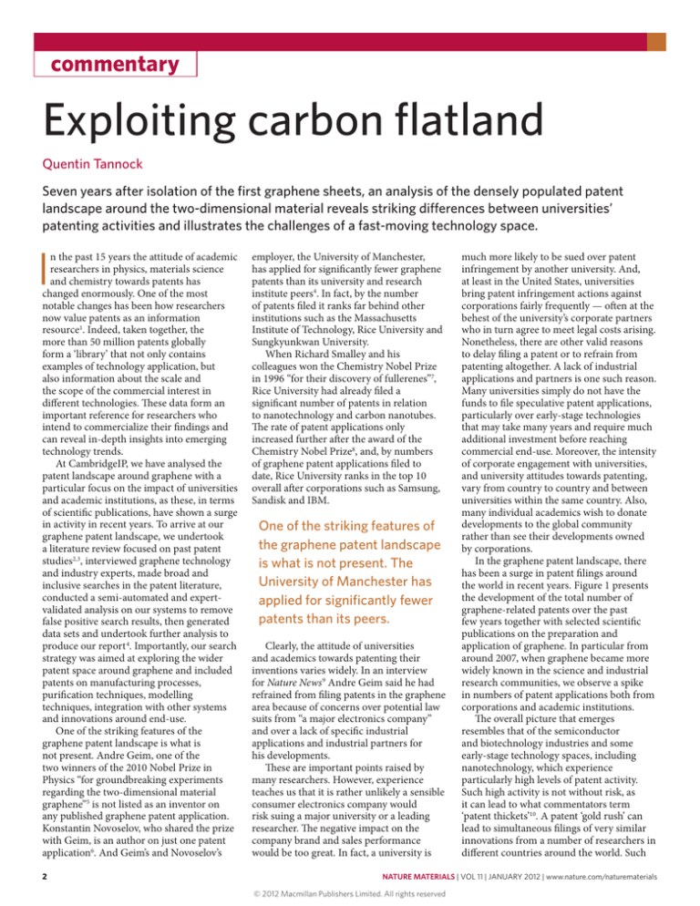
commentary
Exploiting carbon flatland
Quentin Tannock
Seven years after isolation of the first graphene sheets, an analysis of the densely populated patent
landscape around the two-dimensional material reveals striking differences between universities’
patenting activities and illustrates the challenges of a fast-moving technology space.
I
n the past 15 years the attitude of academic
researchers in physics, materials science
and chemistry towards patents has
changed enormously. One of the most
notable changes has been how researchers
now value patents as an information
resource1. Indeed, taken together, the
more than 50 million patents globally
form a ‘library’ that not only contains
examples of technology application, but
also information about the scale and
the scope of the commercial interest in
different technologies. These data form an
important reference for researchers who
intend to commercialize their findings and
can reveal in-depth insights into emerging
technology trends.
At CambridgeIP, we have analysed the
patent landscape around graphene with a
particular focus on the impact of universities
and academic institutions, as these, in terms
of scientific publications, have shown a surge
in activity in recent years. To arrive at our
graphene patent landscape, we undertook
a literature review focused on past patent
studies2,3, interviewed graphene technology
and industry experts, made broad and
inclusive searches in the patent literature,
conducted a semi-automated and expertvalidated analysis on our systems to remove
false positive search results, then generated
data sets and undertook further analysis to
produce our report 4. Importantly, our search
strategy was aimed at exploring the wider
patent space around graphene and included
patents on manufacturing processes,
purification techniques, modelling
techniques, integration with other systems
and innovations around end-use.
One of the striking features of the
graphene patent landscape is what is
not present. Andre Geim, one of the
two winners of the 2010 Nobel Prize in
Physics “for groundbreaking experiments
regarding the two-dimensional material
graphene”5 is not listed as an inventor on
any published graphene patent application.
Konstantin Novoselov, who shared the prize
with Geim, is an author on just one patent
application6. And Geim’s and Novoselov’s
2
employer, the University of Manchester,
has applied for significantly fewer graphene
patents than its university and research
institute peers4. In fact, by the number
of patents filed it ranks far behind other
institutions such as the Massachusetts
Institute of Technology, Rice University and
Sungkyunkwan University.
When Richard Smalley and his
colleagues won the Chemistry Nobel Prize
in 1996 “for their discovery of fullerenes”7,
Rice University had already filed a
significant number of patents in relation
to nanotechnology and carbon nanotubes.
The rate of patent applications only
increased further after the award of the
Chemistry Nobel Prize8, and, by numbers
of graphene patent applications filed to
date, Rice University ranks in the top 10
overall after corporations such as Samsung,
Sandisk and IBM.
One of the striking features of
the graphene patent landscape
is what is not present. The
University of Manchester has
applied for significantly fewer
patents than its peers.
Clearly, the attitude of universities
and academics towards patenting their
inventions varies widely. In an interview
for Nature News 9 Andre Geim said he had
refrained from filing patents in the graphene
area because of concerns over potential law
suits from “a major electronics company”
and over a lack of specific industrial
applications and industrial partners for
his developments.
These are important points raised by
many researchers. However, experience
teaches us that it is rather unlikely a sensible
consumer electronics company would
risk suing a major university or a leading
researcher. The negative impact on the
company brand and sales performance
would be too great. In fact, a university is
much more likely to be sued over patent
infringement by another university. And,
at least in the United States, universities
bring patent infringement actions against
corporations fairly frequently — often at the
behest of the university’s corporate partners
who in turn agree to meet legal costs arising.
Nonetheless, there are other valid reasons
to delay filing a patent or to refrain from
patenting altogether. A lack of industrial
applications and partners is one such reason.
Many universities simply do not have the
funds to file speculative patent applications,
particularly over early-stage technologies
that may take many years and require much
additional investment before reaching
commercial end-use. Moreover, the intensity
of corporate engagement with universities,
and university attitudes towards patenting,
vary from country to country and between
universities within the same country. Also,
many individual academics wish to donate
developments to the global community
rather than see their developments owned
by corporations.
In the graphene patent landscape, there
has been a surge in patent filings around
the world in recent years. Figure 1 presents
the development of the total number of
graphene-related patents over the past
few years together with selected scientific
publications on the preparation and
application of graphene. In particular from
around 2007, when graphene became more
widely known in the science and industrial
research communities, we observe a spike
in numbers of patent applications both from
corporations and academic institutions.
The overall picture that emerges
resembles that of the semiconductor
and biotechnology industries and some
early-stage technology spaces, including
nanotechnology, which experience
particularly high levels of patent activity.
Such high activity is not without risk, as
it can lead to what commentators term
‘patent thickets’10. A patent ‘gold rush’ can
lead to simultaneous filings of very similar
innovations from a number of researchers in
different countries around the world. Such
NATURE MATERIALS | VOL 11 | JANUARY 2012 | www.nature.com/naturematerials
© 2012 Macmillan Publishers Limited. All rights reserved
commentary
a
1,000
Universities/research institutions
Multinationals
SMEs
Other
900
800
700
Patents yearly
600
500
400
300
200
100
b
11
20
10
20
09
20
08
20
07
20
06
20
05
20
04
20
20
03
20
02
20
01
00
20
00
0
Pr
e20
overlapping granted patents can be a reason
for increased litigation, and they have caused
many governments and experts to study the
possible impacts, both positive and negative,
of the patent system on innovation11.
Early signs in the graphene patent area
are positive, with many patent applications
being granted. This is encouraging
as nascent technology areas, such as
nanotechnology, often struggle to arrive
at a coherent terminology for technology
components12. Quite simply, different patent
applicants can call the same component
by different names. Graphene is a 2D form
of crystalline carbon, which gives rise to
additional challenges in distinguishing
it from other forms of nanocarbon in
the patent literature, including carbon
nanotubes and fullerenes. In fact, many
patent authorities even decided to employ
specialist nanotechnology patent examiners
to check nanotechnology applications,
and to create special classification codes.
The European Patent Office, for example,
has already created graphene-specific
patent classifications.
Across all years, there is a relatively high
patent contribution from universities and
research institutes, consistent with other
relatively early-stage and research-intensive
technology spaces. Table 1 highlights
the most active inventors with university
affiliations or collaborations, and shows
strong track records of industry–university
collaborations in both South Korea and
the United States. The contribution of
multinational corporations to the graphene
patent landscape is and remains significant.
There are a number of possible reasons for
this, including the fact that many of the enduse industries for graphene developments
are notoriously patent-intensive. Another
reason may simply be that the material is
perceived as easier to work with and to
scale up than many other nanomaterials,
including carbon nanotubes, that have
seen considerable commercial interest.
And some major corporations have gained
in-house expertise in nanotechnology,
perhaps easing their switch to graphene.
There is evidence in the patent literature of
corporations simply hedging their bets by
adding graphene claims to current patent
families around existing technologies, and
there are signs that some corporations are
engaging in ‘portfolio maximization’ and
‘portfolio optimization’ strategies observed
in information technology, electrical
engineering, biotechnology and other sectors
relying on complex technology systems13. It
has, for example, become relatively common
practice for patents to claim graphene as one
of a long list of potential nanomaterials that
could deliver a desired result.
2004
2006
2007
2009
2010
2010
Electric field
effect in
exfoliated
graphene
Electronic
confinement
in patterned
epitaxial
graphene
Preparation
of graphene
oxide paper
Large-area
synthesis of
graphene on
copper
Roll-to-roll
production of
graphene
films
High-speed
graphene
transistors
with a
nanowire gate
Figure 1 | Development of graphene science and technology. a, The number of patent applications by
year. Patent applications may be unpublished for 18 months or more. Therefore the number of patents for
the past two years may be underrepresented. b, Timeline of some representative scientific discoveries.
Images reproduced from (left to right): ref. 18, © 2004 AAAS; ref. 19, © 2006 AAAS; ref. 20, © 2007 NPG;
ref. 21, © 2009 AAAS; ref. 22, © 2010 NPG; ref. 23, © 2010 NPG.
The largest corporate patent portfolios
in the graphene patent landscape are held
by Samsung and Sandisk, reflecting clear
industrial interests in semiconductorand memory-related applications. Key
differences in corporate research and
development (R&D) focus and commercial
strategies can be inferred from the corporate
patent filings. Samsung has a broad set
of application interests and a wide set of
collaborators including several leading
universities and research institutes around
the world (Fig. 2a). By comparison, Sandisk
has a more highly focused patent portfolio
and relatively few collaborators (Fig. 2b).
Naturally, analysis of the patent data can
reveal R&D collaborations as well as the
focus of specific groups and individuals.
Moreover, individual patent documents can
help readers to identify specifications around
NATURE MATERIALS | VOL 11 | JANUARY 2012 | www.nature.com/naturematerials
© 2012 Macmillan Publishers Limited. All rights reserved
particular industrial applications. Assessing
abandoned patents, comparing journal
articles and the patent literature in specific
spaces, and undertaking analysis of areas
where patents are not filed (‘white space’
or ‘gap’ analysis) can also give researchers
useful clues about ‘dead ends’ to avoid and
areas where commercially viable solutions
are required. Unfortunately, the graphene
patent landscape is not mature enough yet
to show these characteristics reliably, but
they should soon emerge if patenting rates
continue to rise.
As the first 2D crystal discovered, and
with such unusual electronic, optical and
mechanical properties, it is easy to see why
graphene is of such broad interest across
industry fields ranging from semiconductors
to biotechnology. And, like it or not, patents
underpin R&D strategies and commercial
3
commentary
strategies in a great many industries relevant
to graphene research deployments. In the
current economic environment, the chance
of receiving an investment of sufficient
working capital to take a graphene research
project, scale it up and roll out a commercial
application is much less than in the past.
This funding squeeze means that smaller
players are less likely to be able to afford
to ‘do it alone’. Finding corporate strategic
partners with experience, scale and contacts
is now even more important at an even
earlier stage. And, whatever the nature
of the patent landscape in a given area, it
is notoriously difficult for innovators to
assess the possible rewards of taking out a
patent and to balance these against the costs
and risks of doing so. For these and other
reasons, it is leading practice at university
technology-transfer offices to seek corporate
partners as early as possible in the patenting
process. Our graphene patent landscape
indicates that university collaborations
with industry and industrial sponsorship
of university research are common in the
graphene space. There is a high level of
university and corporation graphene patent
co-ownership. Samsung, for example,
co-owns graphene patents with Hanyang
University, Kumoh National Institute
of Technology, Leland Stanford Junior
University, Seoul National University and
Sungkyunkwan University (Fig. 2a).
The chance of an academic
inventor receiving an
investment to roll out a
commercial graphene
application is less than in
the past. Finding corporate
strategic partners is now even
more important.
Many universities have been successful
in developing graphene technologies
themselves and then licensing out patents
covering these technologies to industrial
players. As the World Intellectual Property
Organization says, “licensing not only
creates an income source for the patentee,
but also establishes the legal framework
for the transfer of the technology to a
wider group of researchers and engineers,
who may, in turn, further contribute to
the development of the technology”14.
Massachusetts Institute of Technology, for
example, advertises around 30 graphene
technologies as available for licence on its
Industrial Liaison Program website. And
a search of the Rice University technology
transfer website brings up 14 advertisements
for graphene technology available for
licence, the most recent being for “Growth
of graphene from food, insects, and waste”15.
The UK’s Chancellor of the Exchequer,
George Osborne, has recently announced
a £50 million grant to support UK-based
graphene research and “fund a national
research programme that will take this
Nobel Prize-winning discovery from the
British laboratory to the British factory
floor”16. In response, Konstantin Novoselov
said that the £50 million investment was
“a ‘smart move’ that, if spent wisely, would
Table 1 | Top 10 ranking of university-related inventors by number of patents filed, together with affiliations and example patent titles.
Rank Name
Number
Organizational affiliations in inventor’s
of patents graphene patents
Example patent number
on Boliven.com
Example patent title
1
Jae-young Choi
62
Kumoh National Institute of Technology;
Samsung; Sungkyunkwan University
US20110127497A1
Organic light-emitting device using graphene
2
Hyeon-jin Shin
43
Samsung; Sungkyunkwan University
US20090308520A1
Method for exfoliating carbonization catalyst
from graphene sheet, method for transferring
graphene sheet from which carbonization
catalyst is exfoliated to device, graphene
sheet and device using the graphene sheet
3
Seon-mi Yoon
39
Samsung; Sungkyunkwan University
US20090071533A1
Transparent electrode comprising graphene
sheet, and display and solar cell including
the electrode
4
Ilhan A. Aksay
35
Battelle Memorial Institute; Princeton
University; Vorbeck Materials Corporation
US20100096595A1
Functional graphene–polymer
nanocomposites for gas-barrier applications
5
Hyun-jong Chung
34
Samsung; Seoul National University;
Sungkyunkwan University
US20110089995A1
Graphene device and method of
manufacturing the same
6
Sun-ae Seo
33
Samsung; Seoul National University;
Sungkyunkwan University; Leland Stanford
Junior University
US20110108521A1
Methods of manufacturing and transferring
larger-sized graphene
7
Byung Hee Hong
28
Samsung; Sungkyunkwan University
US20110195207
Graphene roll-to-roll coating apparatus and
graphene roll-to-roll coating method using
the same for graphene
8
Yun-sung Woo
21
Samsung; Seoul National University;
Sungkyunkwan University
US20110108609
Methods of fabricating graphene using
alloy catalyst
9
Robert K.
Prudhomme
21
Princeton University; Vorbeck
Materials Corporation
US20110042813A1
Printed electronics
10
Rodney S. Ruoff
20
Graphene Energy; Northwestern University;
Texas Instruments; University of Texas
WO2008143829A2
Graphene oxide sheet laminate and method
11
James M. Tour
20
University of Texas; William Marsh
Rice University
US20110059871
Graphene compositions and drilling fluids
derived therefrom
12
John S. Lettow
18
Princeton University; Vorbeck
Materials Corporation
US20110049437
Coatings containing functionalized graphene
sheets and articles coated therewith
4
NATURE MATERIALS | VOL 11 | JANUARY 2012 | www.nature.com/naturematerials
© 2012 Macmillan Publishers Limited. All rights reserved
commentary
reap economic dividends”17. Consequently,
whatever the reasons behind the decision
not to file more graphene-related patents
thus far, I expect to see many more
graphene patents from the University of
Manchester and its industrial partners over
the next several years, if only to meet the
expectations of private-sector partners and
public-sector stakeholders. Of course, in
addition to graphene other ‘2D’ materials
exist, and the patent literature could soon
provide evidence of forays into these
new flatlands. Whether you think the
information in patents assists the scientific
discovery process or you feel that the
business interests revealed in patents impede
scientific aims, I am confident that you will
agree with me how fascinating it will be to
observe ‘patenting in the flatlands’ over the
next few years.
❐
a
Kumoh National
Institute of Technology
IUCF-HYU (Industry-University
Cooperation Foundation
Hanyang University)
Seoul National University
Sungkyunkwan University
Hanyang University
Leland Stanford
Junior University
Samsung
Vryus Co. Ltd
Relative No.
of patents
10
Inventor
Assignee
university
Assignee
SME
Assignee
multinational
30
Justus-Liebig-Universitaet
Giessen
100
Quentin Tannock is with CambridgeIP, 8a King’s
Parade, Cambridge CB2 1SJ, UK.
e-mail: quentin.tannock@cambridgeip.com
b
References
University Tsinghua
William Marsh Rice University
Sandisk 3D LLC
Relative No.
of patents
10
Inventor
Assignee
university
Assignee
SME
Assignee
multinational
30
100
c
Drexel University
Trustees of the University of
Pennsylvania
Graphene Energy Inc.
Texas Instruments Inc.
University of Texas
William Marsh Rice University
Lockheed Martin Corporation
Sandisk 3D LLC
Relative No.
of patents
10
Assignee
university
Assignee
SME
Assignee
multinational
30
CAMBRIDGEIP, 2011
Inventor
100
Figure 2 | Graphene patent networks for a, Samsung, b, Sandisk and c, Rice University. The nodes in the
graphs represent individual inventors and organizational assignees such as universities, multinationals, and
small and medium enterprises (SMEs). The lines between the nodes correspond to mutual patent filings.
NATURE MATERIALS | VOL 11 | JANUARY 2012 | www.nature.com/naturematerials
© 2012 Macmillan Publishers Limited. All rights reserved
1. CambridgeIP. Nanotechnology patent survey. http://www.
cambridgeip.com/knowledge-centre/nanotech-survey.html (2011)
2. UK IP Office. A brief analysis of worldwide patent filings
relating to graphene by UK resident applicants and inventors.
http://www.ipo.gov.uk/informatic-graphene-uk.pdf (2011)
3. UK IP Office. An analysis of worldwide patents relating to graphene.
http://www.ipo.gov.uk/informatic-graphene.pdf (2011).
4. CambridgeIP. Patenting flatland: Graphene.
http://www.cambridgeip.com/knowledge-centre/nanotechnology/
graphene.html
5. The Nobel Prize in Physics 2010. http://www.nobelprize.org/
nobel_prizes/physics/laureates/2010/geim.html (2010).
6. Kinloch, I. A., Young, R. J. & Novoselov, K. S. Graphene polymer
composite. WIPO patent WO2011086391A1 (2011).
7. The Nobel Prize in Chemistry 1996. http://www.nobelprize.org/
nobel_prizes/chemistry/laureates/1996 (1996).
8. CambridgeIP. Recent trends in nanotechnology patenting.
http://www.boliven.com/boliven_landscapes/nanotechnology_
patent_review (2011).
9. Brumfield, G. Andre Geim: in praise of graphene. Nature
http://dx.doi.org/10.1038/news.2010.525 (2010).
10.Shapiro, C. Navigating the Patent Thicket: Cross Licenses, Patent
Pools, and Standard Setting, Innovation Policy and the Economy
Vol. 1 (MIT Press, 2000).
11.UK IP Office. Independent review of IP and growth or
‘Hargreaves Review’. http://www.ipo.gov.uk/ipreview.htm (2011).
12.CambridgeIP. Emerging patent thickets and standards in the
medical devices and telehealth space. Innovation, market
dynamics and policy options in cross-over technologies.
http://www.cambridgeip.com/knowledge-centre/keycambridgeip-publications.html (2011).
13.Harfhoff, D. et al. The Strategic Use of Patents and its Implications
for Enterprise and Competition Policies 9–12 (Report
commissioned for the European Commission, 2007).
14.World Intellectual Property Organization. Licensing and
technology transfer, introduction. http://www.wipo.int/patent-law/
en/developments/licensing.html (Accessed 12 November 2011).
15.Rice University. http://rice.flintbox.com/public/project/8867/
(Accessed 19 November 2011).
16.University of Manchester press release. http://www.manchester.
ac.uk/aboutus/news/display/?id=7484 (3 October 2011)
17.Jha, A. The Guardian http://www.guardian.co.uk/science/2011/
oct/07/huge-investment-graphene-nobel-prizewinner
(7 October 2011)
18.Novoselov, K. S. et al. Science 306, 666–669 (2004).
19.Berger, C. et al. Science 312, 1191–1196 (2006).
20.Dikin, D. A. et al. Nature 448, 457–460 (2007).
21.Li, X. et al. Science 324, 1312–1314 (2009).
22.Bae, S. et al. Nature Nanotech. 5, 574–578 (2010).
23.Liao, L. et al. Nature 467, 305–308 (2010).
5
