RF Amplifier Design - Electrical and Information Technology
advertisement
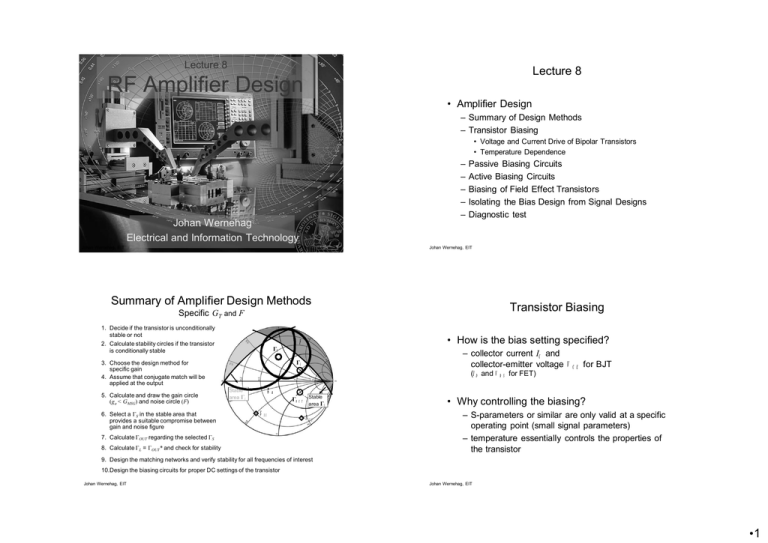
Lecture 8 Lecture 8 RF Amplifier Design • Amplifier Design – Summary of Design Methods – Transistor Biasing • Voltage and Current Drive of Bipolar Transistors • Temperature Dependence – – – – – Johan Wernehag Electrical and Information Technology Passive Biasing Circuits Active Biasing Circuits Biasing of Field Effect Transistors Isolating the Bias Design from Signal Designs Diagnostic test Johan Wernehag, EIT Johan Wernehag, EIT Summary of Amplifier Design Methods Transistor Biasing Specific GT and F 1. Decide if the transistor is unconditionally stable or not 2. Calculate stability circles if the transistor is conditionally stable 3. Choose the design method for specific gain 4. Assume that conjugate match will be applied at the output (ID and VDS for FET) Stable area 6. Select a S in the stable area that provides a suitable compromise between gain and noise figure OUT 8. Calculate L = regarding the selected OUT* – collector current IC and collector-emitter voltage VCE for BJT L 5. Calculate and draw the gain circle (ga < GMSG) and noise circle (F) 7. Calculate • How is the bias setting specified? F S ga S OUT S11 Stable area S22 S and check for stability L • Why controlling the biasing? – S-parameters or similar are only valid at a specific operating point (small signal parameters) – temperature essentially controls the properties of the transistor 9. Design the matching networks and verify stability for all frequencies of interest 10.Design the biasing circuits for proper DC settings of the transistor Johan Wernehag, EIT Johan Wernehag, EIT •1 Voltage or Current Drive of the Transistor The collector current increase exponentially wrt the base voltage • Voltage drive: Voltage Drive of Bipolar Transistors • Simplified relationship: IC – where the thermal voltage VBE • k = Boltzmann’s constant = 1.38·10-23 [J/K] • T = absolute temperature [K] • q = charge of the electron = 1.6·10-19 [C] The collector current depends linearly wrt the base current • Current drive: IC • The saturation current IS varies between different transistors • VT and IS are temperature dependent IB Johan Wernehag, EIT Johan Wernehag, EIT Temperature Dependence at Voltage Driven Biasing Temperature Dependence at Current Driven Biasing 80mA 55 A • Example: Calculate the collector current at constant VBE -20 to 80 is a standard temp. range for a commercial design Johan Wernehag, EIT The temperature dependence at current driven biasing is considerably ”friendlier” compared to voltage driven biasing! A factor of 2 compared to 10million! Johan Wernehag, EIT •2 Controlling the Operating Point • The operating point needs to be controlled to avoid thermal avalanche effect that might destroy the device • Three common methods to implement the feedback: Current Driven Biasing • The simplest circuitry: – Moderate temperature dependency – Sensitive to variations in the current gain, – Requires large resistance values 0 – Loop gain: – Large loop gain if the ratio VCC / VCE is large – passive current or voltage driven biasing – active biasing • Alternative circuit solution: – – – – Not strictly current driven Moderate temperature dependency Less sensitive to variations in the current gain Does not require large resistance values – Loop gain : – thermal feedback Johan Wernehag, EIT – Large loop gain if the ratio VCC / VCE is large Johan Wernehag, EIT Voltage Driven Biasing Example of Active Biasing Circuit • Series feedback without feedback • Decent temperature dependence • Not sensitive to variations in the current active biasing gain passive current drive • RC may be replaced with an RFC* • Loop gain: gm·RE • Not suitable at high frequencies – due to difficulties to signal ground the emitter without introducing stability problems T2: low frequency transistor working as current generator T1: high frequency transistor *RFC = Radio-Frequency Choke, a large reactance coil intended for high frequencies Johan Wernehag, EIT Johan Wernehag, EIT •3 Control by Thermal Feedback Biasing of Field Effect Transistors • The FET shows a slight temperature dependence compared to the BJT • Large spreading in the threshold voltage compared to the BJT Thermally connected • Only voltage driven biasing possible • Passive biasing circuits are not usable if there is a large variation in the threshold voltage The diode VD is thermally connected to the transistor Good in PAs etc. where high currents heat it up Johan Wernehag, EIT Johan Wernehag, EIT Isolating the Bias Design from the Signal Design Example using RFC’s Isolating the Bias Design from the Signal Design Example using stubs biasing circuit biasing circuit signal output signal output signal input signal input signal circuit RFC = Radio-Frequency Choke may be used up to medium high frequencies Johan Wernehag, EIT signal circuit At high frequencies the RFC’s are replaced with line elements Johan Wernehag, EIT •4 Lab 3 – RF amplifier Johan Wernehag, EIT •5
