DAC100 10-Bit Current Output D/A Converter Data Sheet (Rev. D)
advertisement
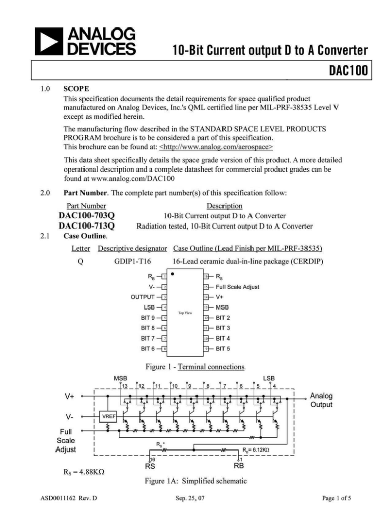
DAC100 3.0 3.1 10-Bit Current output D to A Converter Absolute Maximum Ratings. (TA = 25°C, unless otherwise noted) V+ supply to V- supply.........................................................................................0V to 36V V+ supply to output ........................................................................................... 0V to +18V V- supply to output .............................................................................................0V to –18V Power dissipation ......................................................................................................500mW Logic inputs to outputs........................................................................................ -1V to +6V Operating temperature range...................................................................... -55°C to +125°C Storage temperature range ......................................................................... -65°C to +150°C Lead temperature (soldering, 60 sec.)....................................................................... +300°C Dice junction temperature (TJ)................................................................... -65°C to +175°C Thermal Characteristics: Thermal resistance, CERDIP (Q) Package Junction-to-case (ΘJC) = 29°C/W Max Junction-to-ambient (ΘJA) = 91 °C/W Max Thermal resistance, FLATPAK (N) Package Junction-to-case (ΘJC) = 22°C/W Max Junction-to-ambient (ΘJA) = 90 °C/W Max Electrical Table: See notes at end of table TABLE I Parameter Symbol Conditions 1/ Subgroup Power supply current I+ VIH = 2.1V IFull range output voltage Limit Min Limit Max Units 1, 2, 3 8.33 mA VIH = 2.1V 1, 2, 3 8.33 VFR VIL = 0.7V, Full Adjust pin tied to V- 1, 2, 3 Zero scale output voltage VZS VIH = 2.1V Integral nonlinearity NL Full scale temperature coefficient TCVFR Logic inputs high VIH Logic inputs low VIL Logic input current high 11.1 V 1, 2, 3 ±.013 %FS ± ½ LSB – 9 Bits 1, 2, 3 ±0.1 8 ±60 IIH VIL = 0.7V, Full Scale Adjust pin tied to VVIN = 2.1V to 3V (all inputs) Measured with respect to output pin allowing ≤ ±½ LSB change with ΔVIN VIN = 0.7V to 0V (all inputs) Measured with respect to output pin allowing ≤ ±½ LSB change with ΔVIN VIH = 6.0V, Each Input Logic input current low IIL Power supply sensitivity 1, 2, 3 10.0 2.1 V 1, 2, 3 0.7 1, 2, 3 5 VIL = 0V, Each Input 1, 2, 3 5 PSS VIL = 0.7V (all inputs) VS = ±6V to ±18V 1, 2, 3 ±0.1 Monotonicity 2/ ΔIO Measured at each major carry code point 1 Settling time 3/ TSHL RL = 1KΩ, CL ≤ 10pF 9 ASD0011162 Rev. D Sep. 25, 07 ppm/° C μA %/V μA 0 375 nS Page 2 of 5 DAC100 10-Bit Current output D to A Converter Table I notes: 1/ VS = ±15V, unless otherwise specified. 2/ The change in output current either increases or remains the same for an increasing digital input code. 3/ Output within ± ½ LSB of 10-bit accuracy final settled nominal value of VOUT. Input pulse characteristics: Input frequency = 1MHz square wave, 50% duty cycle. Input amplitude = 0V to 2.1V Input signal = tr, tf ≤ 20 nS Measurement referenced to input High-to-Low Transition. DUT Settling Time to ±0.05 % FS 4.1 Electrical Test Requirements: Table II MIL-STD-883 Test Requirements Subgroups (see table I) Interim electrical parameters (pre Burn-In) 1 Final Electrical Test Parameters 1, 2, 3, 8 1/ 2/ Group A Test Requirements 1, 2, 3, 8, 9 Group C Test Requirements 1 Group D Test Requirements 1 * PDA applies to Subgroup 1 only. No other subgroups are included in PDA. 1/ PDA applies to subgroup 1. Deltas not included in PDA 2/ See table III for deltas. See table I for test conditions. 4.2 Table III. Burn-in test delta limits. TEST TITLE BURN-IN ENDPOINT Table III LIFETEST ENDPOINT VFR 10.55 ± 0.55 10.55 ± 0.75 ±0.2 V VZS ±0.013 ±0.018 ±0.005 %FS I+ 8.33 8.33 ±10% mA I- 8.33 8.33 ±10% mA ASD0011162 Rev. D Sep. 25, 07 DELTA LIMIT UNITS Page 3 of 5 DAC100 5.0 10-Bit Current output D to A Converter Life Test/Burn-In Circuit: HTRB is not applicable for this drawing. 5.1 5.2 Burn-in is per MIL-STD-883 Method 1015 test condition B. 5.3 Steady state life test is per MIL-STD-883 Method 1005. ASD0011162 Rev. D Sep. 25, 07 Page 4 of 5 DAC100 Rev A B C D 10-Bit Current output D to A Converter Date Initiate 30-Jun-00 Update web address Feb. 18, 2002 Update web address. Add Group C and D to table II. Add life test Feb. 28, 2003 endpoint based on delta to table III. Delete Burn-In circuit Aug. 5, 2003 ASD0011162 Rev. D Description of Change Sep. 25, 07 Page 5 of 5

