Broadband SiGe Monolithic Microwave Control Circuits
advertisement
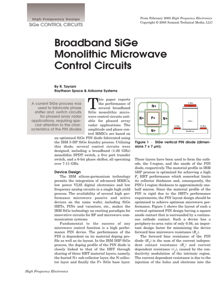
From February 2005 High Frequency Electronics Copyright © 2005 Summit Technical Media, LLC High Frequency Design SiGe CONTROL CIRCUITS Broadband SiGe Monolithic Microwave Control Circuits By R. Tayrani Raytheon Space & Airborne Systems T his paper reports the performance of several broadband SiGe monolithic microwave control circuits suitable for phased array radar applications. The amplitude and phase control MMICs are based on an optimized SiGe PIN diode fabricated using the IBM 5-HP SiGe foundry process. Utilizing this diode, several control circuits were designed, including a broadband (1-20 GHz) monolithic SPDT switch, a five port transfer switch, and a 6-bit phase shifter, all operating over 7-11 GHz. A current SiGe process was used to fabricate phase shifter and switch circuits for phased array radar applications, requiring special attention to the characteristics of the PIN diodes Device Design The IBM silicon-germanium technology permits the integration of advanced MMICs, low power VLSI digital electronics and low frequency analog circuits in a single high yield process. The availability of several high performance microwave passive and active devices on the same wafer, including SiGe HBTs, PINs and varactors, etc., makes the IBM SiGe technology an exciting paradigm for innovative circuits for RF and microwave communication systems. Fundamental to the success of any microwave control function is a high performance PIN device. The performance of the PIN is dependent on its material doping profile as well as its layout. In the IBM 5HP SiGe process, the doping profile of the PIN diode is closely linked to that of the HBT through sharing of three HBT material layers, namely, the buried N+ sub-collector layer, the N-collector layer and finally the P+ SiGe base layer. High Frequency Electronics Figure 1 · SiGe vertical PIN diode (dimensions 7 x 7 µm). These layers have been used to form the cathode, the I-region, and the anode of the PIN diode, respectively. The material profile in IBM 5HP process is optimized for achieving a high Ft HBT performance which somewhat limits its collector thickness and, consequently, the PIN’s I-region thickness to approximately onehalf micron. Since the material profile of the PIN is rigid due to the HBT’s performance requirements, the PIN layout design should be optimized to achieve optimum microwave performance. Figure 1 shows the layout of such a vertical optimized PIN design having a square anode contact that is surrounded by a continuous cathode contact. Such a device has a periphery-to-area ratio of only 0.56, an important design factor for minimizing the device forward bias microwave resistance (Rƒ). The forward bias resistance of the PIN diode (Rƒ) is the sum of the current independent contact resistance (Rc) and current dependent resistance (rƒ), caused by the conductivity modulation of the intrinsic region. The current dependent resistance is due to the injection of the holes and electrons into the High Frequency Design SiGe CONTROL CIRCUITS Figure 2(a) · Shunt SiGe PIN diode across 50 ohm CPW lines. Figure 2(b) · Measured and modeled (using ICCAP) DC-IV characteristics of the shunt diode (80). Figure 2(d) · Microwave performance of series and shunt diodes (If = 2 mA, Vf = 1.0V, Vr = –1 V). PIN Area µm2 IL (dB) 10 GHz Iso. (dB) 10 GHz Cj (fF) –1 V Rf (W ) Vf = 1 V 80 Shunt 0.5 18.0 32 3.5 @ 2 mA 50 Series 0.7 18.0 20 9.0 @ 2 mA Table 1 · Measured performance and extracted Cj and Rf values. intrinsic region from the forward biased P+ and N+ contact regions. This resistance is given by: (1) – is Where li is the thickness of the intrinsic region; µ the average electron and hole mobility; and (t) is the minority carrier life time. Device Performance Figure 2(a) illustrates a fully fabricated 80 µm2 shunt device in a 50 ohm system. As it can be seen, the buried High Frequency Electronics Figure 2(c) · Measured and modeled (using ICCAP): log I (A) vs. voltage (V). Figure 2(e) · Measured and modeled (using ADS) performance of an integrated series-shunt diode (If = 2 mA, Vf = 1.0 V, Vr = –1 V). PIN is accessed by six vias that connect the device terminals to the input-output launching pads. The transmission lines are formed on a 15-micron thick polyimide layer that is deposited on the surface of the SiGe substrate. Good agreement has been obtained between the modeled and the measured DC current-voltage characteristics of the diode as shown in Figures 2(b) and 2(c). The diode follows a parallel plane diode behavior, given by Eq. (2), over seven orders of magnitudes. (2) The measured and modeled data on saturation current (Is), the ideality factor (n), and the junction revere breakdown voltage (Vb) are found to be: Is = 1.2 x 10⁻¹⁷, n = 1.1 at T = 300K, and Vb = 18 V. The value of (n) has a significant effect on the performance of the PIN diode [1-3]. Figure 2(d) illustrates the RF performances for typical 50 µm2 and 80 µm2 diodes when placed across or in series with 50 ohm CPW input-output transmission lines. As can be seen, good broadband performance has been obtained for both series and shunt devices at a low dissi- High Frequency Design SiGe CONTROL CIRCUITS Figure 3(a) schematic. · SPDT switch chip pation power of 2.0 mW. Table 1 summarizes the extracted values for junction capacitance and the total forward biased resistance (Rƒ) for both devices. The measured and modeled performance for a typical integrated seriesshunt diode pair (50 series, 80 shunt) is shown in Figure 2(e). To achieve a broadband RF operation for this structure, the distance between the two diodes was set to approximately 10, thereby minimizing its associated parFigure 3(b) · SiGe SPDT switch chip asitics. (1.0 × 0.42 mm). Broadband (1 to 20 GHz) SPDT Switch The series-shunt integrated diode structure described above was used to design a broadband SPDT switch with on-chip resistive biased networks that operates over 1 to 20 GHz bandwidth. All aspects of the circuit design and device modeling were performed using Agilent ADS simulators [4]. Figure 3(a) shows the SPDT switch schematFigure 3(c) · Measured and mod- Figure 3(d) · Switch input power at ic having a series-shunt diode combieled (using ADS) SPDT switch per- 1-dB compression. nation in each arm. This topology was formance. chosen as the best compromise between minimizing the insertion loss and maximizing the switch isolation. On-chip resistive bias networks were also employed to ensure broadband switching performance and smaller chip size as illustrated in Figure 3(b). The 1500 ohm bias resistors in this design use 340 ohms per square polysilicon thin film resistors and the MIM capacitors are based on 0.7 fF/µm2 thin dielectric film (SiO2) capacitors. Referring to Figure 3(a), a throughpath between ports 1 and 2 exists when Vb2 = –6.8V and Vb1 = 0, causing the series diode to become forward biased at 2 mA while the shunt diode is reversed biased. Figure 4(a) · Transfer switch schematic. Similarly, an isolation path exists between ports 1 and 3 when Vb3 is set at (3.8 V, 2 mA). The total DC power consumption for this design is only around 22 mW for a typical switch. As shown in Figure 3(c), a through-path loss of 0.9 to 1.3 dB and an isolation path loss of 60 to 40 dB over a wide frequency range (1 to 20 GHz) have been measured. Also shown is the close agreement obtained between the switch measured and simulated data. A similar chip without the on-chip resistive bias networks was also measured, requiring only 4.0 mW of DC power for maintaining the same switch performance. The input port power handling capability of the switch is shown in Figure 3(d) indicating the 1-dB insertion loss Figure 4(b) · Transfer switch chip (3.2 × 1.4 mm). compression point occurs at around 19 dBm when meaHigh Frequency Electronics High Frequency Design SiGe CONTROL CIRCUITS Figure 5(a) · Switch measured insertion loss and isolation. Figure 5(b) return loss. · Figure 6 · 180/90 degrees and 45/22.5 degrees phase 2-bit schematic. Figure 7 · 11.25/5.625 degrees phase bit schematic. sured under the nominal bias condition described above. The switching speed and the third order intercept point were both evaluated at 10 GHz. The switching speed was found to be less than one nanosecond and the third order intercept point around 30 dBm at –3 dBm input RF power. X-band SiGe MMICs IBM’s SiGe BiCMOS 5HP process offers the potential to integrate high levels of microwave circuitry with analog and digital circuits. Microwave functions traditionally High Frequency Electronics performed by gallium arsenide MMICs can now be combined with the analog/digital functions of silicon based ASICs on a single chip. As an example of higher microwave integration levels, several X-band SiGe MMICs, including a transfer switch, a 6-bit phase shifter, a 5-bit attenuator and a variable gain cascode amplifier, is described in this section. The post SiGe topside process is described in Switch measured details in the section “Topside Polyimide Technology.” Transfer Switch—Figure 4(a) shows the circuit schematic of a 5-port transfer switch containing 10 optimized SiGe PIN diodes. The circuit design is suitable for applications where Common Leg Circuit (CLC) architecture [5] is employed for the realization of phased array T/R modules. In the CLC topology, the transfer switch would enable the amplifier gain control and phase control circuitries to be shared by both transmit and receive signal paths. The switch design is based on a series-shunt 50 diode combination as the best compromise between minimizing the insertion loss and maximizing the switch isolation. The simplicity of the circuit design is the result of the low parasitic capacitance and resistance of the SiGe PIN diodes leading to a compact chip size shown in Figure 4(b). The switch measured insertion loss, isolation, and return loss are shown in Figures 5(a) and 5(b). The transfer switch demonstrates a path loss of 1.4 to 2.1 dB and an isolation of >55 dB across 7 to 11 GHz. The measured input and output return losses are better than 10 dB over the same frequency band (Figure 5(b)). 6-bit Phase shifter—The phase shifter design consists of six digital bits (180, 90, 45, 22.5, 11.25 and 5.625 degrees) cascaded in a linear arrangement. This provides 64 phase states between 0 and 360 degrees, in increments of 5.625 degrees. The 180, 90, 45 and 22.5 degree phase bits switch between Pi- and/or T-type high-pass/low-pass phase shift networks using two single pole double throw PIN diode switches. The 11.25 and 5.625 degree phase bits use a simplified topology of capacitive and inductive elements to achieve their phase shifts [6]. These phase bit topologies are selected due to their broad bandwidth performance and relative insensitivity to process variations. The schematics for these phase bit circuits are shown in Figures 6 and 7. SiGe PIN diodes (7 × 7 mm) are used for switching functions. Diode biasing is provided through spiral inductors in combination with MIM bypass capacitors. The 180, 90, 45 and 22.5 degree phase bits require two complementary bias inputs of ±1 V. The 11.25 and 5.625 degree phase bits use the same voltages but require a single bias input. High Frequency Design SiGe CONTROL CIRCUITS Figure 8(a) · 6-bit phase shifter chip (3.8 × 3.8 mm). Figure 8(b) · The completed 6-bit phase shifter chip and its associated circuit topology are shown in Figures 8(a) and 8(b). Programmable current sources were used to bias each onstate diode at 2.5 mA. Total current for the phase shifter was 45 mA. Figures 9 through 11 summarize the measured performance of the primary phase states over 5 to 15 GHz, where 7 to 11 GHz is the design band. In the reference state, all phase bits were switched to their highpass state. At 9 GHz, the measured output 1 dB gain compression is 3 dBm with a TOI of 17 dBm. Post measurement simulations indicate that the overall circuit performance can be improved with additional topside technology improvement leading to improved circuit loss for spiral inductors, transmission lines and input/output (I/O) connections of the phase shifter. Topside Polyimide Technology The present IBM SiGe BiCMOS IC process is based on Figure 9 · Measured phase shifter insertion loss. High Frequency Electronics conductive silicon substrates. Therefore, to realize a low loss medium for transmission lines (TRLs), a topside polyimide process has been developed. In the standard IBM 5HP SiGe process, there are five levels of AlCu interconnect metalization. The top-most layer of this metal system is used as a RF ground-plane for the microstrip transmission lines in a polyimide process. Such a groundplane must have openings to allow connections 6-bit phase shifter circuit. between the TRLs above and the active and passive devices below. The first step to create MMICs from the completed Si wafers is to deposit a polyimide layer on top of the ground-plane metalization layer (top metal). After polyimide deposition, vias are etched to contact devices below the ground plane. The polyimide thickness is 15 microns. Figure 12 shows the cross-sectional view of the IBM Si based MMICs using microstrip TRLs on polyimide. As shown in Figure 13, the transmission line loss for a typical 50 ohm microstrip line on polyimide is about 1.20 dB/cm at 10 GHz. Conclusion The design and measured performance of several broadband SiGe MMICs including a broadband (1 to 20 GHz) monolithic SPDT switch, a five port transfer switch, and a 6-bit phase shifter, all operating over 7 to 11 GHz, are described. The amplitude and phase control MMIC designs are based on an optimized SiGe PIN diode. The broadband Figure 10 · Measured phase shifter phase performance. Figure 11 · Measured phase shifter input return loss. Figure 12 · Cross-sectional view of the topside process. Figure 13 · Loss vs. frequency for 50 ohm, 1 cm TRLs on 15.0 µm polyimide. (1-20 GHz) resistive bias SPDT switch “ON” arm demonstrates a path-loss of less than 1.3 dB while its “OFF” arm maintains an isolation of greater than 40 dB across 1 to 20 GHz while consuming only 22 mW of DC power. The switching speed, the 1-dB insertion loss compression point and the third order intercept point were found to be <1 ns, 19 dBm and 30.0 dBm, respectively. The transfer switch is a five port design containing 10 PINs and demonstrates a path loss of 1.4 to 2.1 dB across 7 to 11 GHz, the isolation over the same band is >55 dB. The 6-bit phase shifter design successfully demonstrates the feasibility of using SiGe technology for microwave phase control circuit designs. The availability of high performance PIN diodes and other microwave devices including SiGe HBTs, varactors, etc., renders the IBM SiGe technology a new and exciting paradigm for innovative circuit designs suitable for RF and microwave communication systems. 258. 4. Agilent Advanced Design Systems (ADS 2003) and Agilent ICCAP, V.5.4. 5. A.D. McLachlan and M. Rhodes, “Vector control for airborne phased array radra,” IEE special issue on phased array radar, 1989. 6. M. Teshiba, et al., “A SiGe MMIC 6-Bit PIN Diode Phase Shifter,” IEEE November 2002 MWCL. References 1. J.F. White, Semiconductor Control, Artech House. 2. R. Tayrani, et al., “X-band SiGe monolithic control circuits,” IEEE Topical Meeting on Silicon Monolithic Integrated Circuits in RF Systems, 1998, pp. 126-134. 3. R. Tayrani, et al., “A Broadband (1-20 GHz) SiGe Monolithic SPDT Switch,” IEEE GaAs IC Symposium Technical Digest, Oct. 2002, pp. 255- Author Information Reza Tayrani received the B.Sc, M.Sc and Ph.D. degrees in electrical engineering from Kent University, Canterbury, England in 1974, 1977 and 1985, respectively. He is currently an Engineering Fellow at Raytheon Microwave Center, Space & Airborne Systems, El Segundo, CA. Dr. Tayrani has over 23 years of experience in the areas of GaAs and SiGe MMICs and their related device and technology development. He has designed and developed many MMICs based on MESFETs, HEMTs, pHEMTs, and HBTs for microwave and millimeter-wave applications. His current areas of interests are high efficiency switching mode monolithic power amplifiers, advanced SiGe MMICs, broadband sampling circuits and miniature switched filters. Dr. Tayrani has published over 48 technical papers and holds 7 patents. He can be reached by e-mail at rtayrani@raytheon.com
