VOL. 11, NO. 5, MARCH 2016
ARPN Journal of Engineering and Applied Sciences
ISSN 1819-6608
©2006-2016 Asian Research Publishing Network (ARPN). All rights reserved.
www.arpnjournals.com
DESIGN OF SPDT SWITCH WITH TRANSMISSION LINE STUB
RESONATOR FOR WIMAX AND LTE IN 3.5 GHZ BAND
1Centre
N. A. Shairi1, Z. Zakaria1, A. M. S. Zobilah1, B. H. Ahmad1 and P. W. Wong2
for Telecommunication Research & Innovation (CeTRI), Faculty of Electronics and Computer Engineering,
UniversitiTeknikal Malaysia Melaka (UTeM), Hang Tuah Jaya, Durian Tunggal, Melaka, Malaysia
2Department of Electrical & Electronic Engineering, UniversitiTeknologi PETRONAS (UTP),
Bandar Seri Iskandar, Tronoh, Perak, Malaysia
E-Mail: noorazwan@utem.edu.my
ABSTRACT
A Single Pole Double Throw (SPDT) switch design with transmission line stub resonator for application of
WiMAX and LTE in 3.5 GHz band is proposed in this paper. The transmission line stub resonator is an open stub with
quarter wave of the electrical length. A PIN diode was used in the resonator to reconfigure the resonator between bandstop
and allpass responses. The implementation of the transmission line stub resonators in SPDT switch design was discussed
together with the circuit operation. The result showed that the isolation of SPDT switch with transmission line stub
resonator was higher than 30 dB in the 3.5 GHz band compared to the conventional design and it was verified with
measurement results.
Keywords: RF switch, SPDT, resonator, transmission line stub, switchable resonator, bandstop to allpass.
INTRODUCTION
In Time Division Duplex (TDD) communication
systems such as WiMAX [1] and LTE [2], Single Pole
Double Throw (SPDT) switch is commonly used in RF
front-end system to switch between transmitter [3] and
receiver [4]. This allows a switching between uplink
(transmit mode) and downlink (receive mode) for data
transmissions. As illustrated in Figure-1, in the RF frontend system, the SPDT switch is a part of other
subcomponents such as amplifier [5], [6] , low noise
amplifier (LNA) [7] and antenna [8].
To minimize any RF power leakage between the
transmitter and receiver, high isolation (especially for high
power application) is the key parameter in SPDT switch
design. Therefore, discrete PIN diodes are still desirable
for this higher power application used in military, satellite
communication or base station applications [9].
Figure-1. SPDT switch in RF front-end system.
For low frequencies application especially in Lband (1 - 2 GHz) and S-band (2 - 4 GHz) [10], the discrete
PIN diodes are usually in standard packaging such as
SOT23, SOT323, SOD323 or SOD523 [11], [12].
However, it is difficult to get isolation higher than 25 dB
(for applications above 3 GHz) if using only single
discrete PIN diodes in SPDT switch design.
On the other hand, there are several techniques of
isolation improvements such as material with fabrication
process design, circuit design, resonant circuit,
transmission line and resonator [13]. Most of these
techniques were applied in SPST and Single Pole Multi
Throw (SPMT) switches. In general, resonators can be
used in several circuit designs such as filter [14], [15],
microwave absorber [16], amplifier [5] and antenna [17],
[18].
In this paper, a transmission line stub resonator is
proposed in SPDT switch design for application of
WiMAX and LTE in 3.5 GHz band. By using this
resonator, high isolation was obtained compared to
conventional single shunt SPDT switch.
Transmission line stub resonator
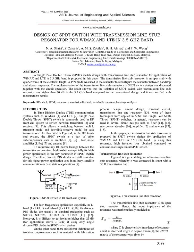
Figure-2 is a general diagram of transmission line
stub resonator, whereby it was connected in shunt with a
50 Ω transmission line.
Figure-2. Transmission line stub resonator.
The transmission line stub resonator is an open
stub resonator. Hence, the input impedance of the
resonator was mathematically modeled as
(1)
where Zs is characteristic impedance of resonator
and θs is electrical length in degree. From (1), the ABCD
matrix of the resonator was given by
3198
VOL. 11, NO. 5, MARCH 2016
ARPN Journal of Engineering and Applied Sciences
ISSN 1819-6608
©2006-2016 Asian Research Publishing Network (ARPN). All rights reserved.
www.arpnjournals.com
(2)
The transmission line stub resonator is a reciprocal
and symmetrical network, whereby S12 = S21. Therefore,
the S12 and the S21 of the resonator were obtained by
converting the ABCD matrix in (2) to S-parameter. Hence,
(b)
(3)
Consider a normalized characteristic of impedance
where Z0 = 1 and impedance of resonator, Zs = Z0 = 1. In
order to produce attenuation or notch response of the
resonator, the electrical length was θs = 90° (or π/2 radian).
Hence, the S-parameter of (3) becomes,
(4)
or in decibel
(5)
From (5), an ideal infinite attenuation or notch were
obtained when the electrical length of the open stub
resonator was a quarter wave (λ/4). In degree and radian,
they were 90° and π/2 radian respectively. These
attenuation characteristics were used to produce high
isolation of SPDT switch.
To allow transmit and receive mode switching
operation in SPDT switch, the transmission line stub
resonator was attached with a PIN diode as illustrated in
Figure-3(a). The PIN diode was connected in between the
microstrip line and stub resonator, hence the switchable
stub resonator could be performed by giving a different
biasing voltage. As depicted in Figure-3(b), if a positive
voltage was applied (+5 V), the PIN diode, D would be in
the ON state and the transmission line stub resonator
would be connected to the microstrip line. In this
condition, it operated as a bandstop filter due to the quarter
wave (λ/4) line of the open stub resonator, converting from
an open to short circuit to the main microstrip transmission
line. If a negative voltage (-5 V) was applied (as shown in
Figure-3(c)), D would be in the OFF state and the
transmission line stub resonator would be disconnected
from the microstrip line. In this condition, the transmission
line stub resonator responded as an allpass between Port 2
and Port 1.
(a)
(c)
Figure-3. Circuit diagram of switchable transmission line
stub resonator. Circuit operation: (b) ON state (bandstop
response) and (c) OFF state (allpass response).
SPDT Switch design
Conventional single shunt SPDT switches was
designed (as shown in Figure-4(a)) for isolation
performance comparison to the proposed SPDT switch
with transmission line stub resonator. A quarter
wavelength of transmission line (λ/4) was used in order to
transform the short circuit (created by the ON state of
shunt PIN diode) to an open circuit at transmit and receive
transmission line junctions. For example, during transmit
mode, the transmitted RF signals from Port 1 to Port 2
would see high impedance at this transmission line
junction. Hence, there would be almost no RF leakage
from Port 1 to Port 3.
(a)
(b)
Figure-4. (a) Circuit diagram of conventional shunt SPDT
switch; and (b) Circuit operation during transmit mode.
Figure-4(b) is the circuit operation of single shunt
SPDT discreet switch. Since the circuit of SPDT switch is
symmetrical, this paper discusses the operation in transmit
mode only. Hence, during transmit mode operation, D1
must be turned OFF and D2 must be turned ON with
Vbias1 = - 5 V and Vbias2 = + 5 V. In this condition, the
RF signals propagated from Port 1 (Transmit) to Port 2
(Antenna) that was measured as insertion loss. The
3199
VOL. 11, NO. 5, MARCH 2016
ISSN 1819-6608
ARPN Journal of Engineering and Applied Sciences
©2006-2016 Asian Research Publishing Network (ARPN). All rights reserved.
www.arpnjournals.com
transmit arm should produce very low RF signal losses.
The isolation between Port 3 (Receive) and Port 1
(Transmit) was obtained from the ON state of PIN diode
(D2) in the receive arm.
Figure-5 shows SPDT switch with transmission
line stub resonator. In each arm (transmit and receive
circuits), the switchable transmission line stub resonators
(S1 and S2) were cascaded with conventional single shunt
SPDT switch. They were spaced with quarter wave (λ/4)
line to convert from low impedance of transmission line
stub resonator to high impedance in the microstrip line.
ADS, all the FR4 substrate parameters were included in
the circuit design having thickness of 1.6 mm and relative
dielectric constant, εr of 4.7. The commercial PIN diodes
(part number: BAP64-02) from NXP were used in the
circuit design. Through a simulation process, the final
dimensions of transmission line stub in the SPDT discrete
switch design were determined together with the parasitic
effect of the PIN diode model. This means that the
parameters of PIN diode such as junction capacitance (Cj)
and series inductance (Ls) were taken into account in the
resonator design. Therefore, the final dimensions of the
resonator were W = 7 mm and l = 5.25 mm. The prototype
of the SPDT switch circuit is shown in Figure-6. The total
area of the circuit was 57 mm x 20 mm.
Figure-5. Circuit diagram of SPDT switch with
transmission line stub resonator.
During transmit mode operation, the D2 and PIN
diode of S2 were turned ON with voltage control of +5 V,
and D1 and PIN diode of S1 were turned OFF with voltage
control of -5 V. In this condition, the S1 produced an
allpass response and RF signals with low insertion loss
propagated from Port 1 (Transmit) to Port 2 (Antenna).
The switchable transmission line stub resonator (S2) in
receive arm (Port 3) acted as a bandstop filter, hence
produced an additional isolation in the SPDT switch.
Table-1 summarizes the circuit operation during
transmit and receive modes of SPDT switch with
transmission line stub resonator for WiMAX and LTE in
3.5 GHz band.
Table-1. Summary of circuit operation of SPDT switch
with switchable transmission line stub resonator.
The SPDT switch with transmission line stub
resonator circuit in Figure-5 was constructed in Advanced
Design System (ADS) software for performance
simulation and layout design. Using microstrip model in
Figure-6. Prototype of SPDT switch with switchable
transmission line stub resonator.
Simulation and measurement results
Figure-7 shows the simulated and measured
results of conventional single shunt SPDT switch in 3.5
GHz band (3.4 to 3.6 GHz). In general, both simulated and
measured results were comparable to each other. As
shown in Figure-7(a), the insertion loss, S21 was from 0.76
to 0.77 dB in simulation and from 1.28 to 1.29 dB in
measurement. Meanwhile, the simulated isolation, S31 as
shown in Figure 7(b) was from 8.9 to 8.5 dB while the
measured isolation was from 7.8 to 7.4 dB. It showed that
the isolation of single shunt PIN diode (in discrete
packaged form) was very low and insufficient to isolate
high RF power leakage between transmitter and receiver
in the RF front-end system.
(a)
3200
VOL. 11, NO. 5, MARCH 2016
ISSN 1819-6608
ARPN Journal of Engineering and Applied Sciences
©2006-2016 Asian Research Publishing Network (ARPN). All rights reserved.
www.arpnjournals.com
(b)
(b)
Figure-7. Simulated and measured results of conventional
SPDT switch, (a) insertion loss (S21), (b) isolation (S31).
Figure-8. Simulated and measured results of SPDT switch
with transmission line stub resonator, (a) insertion loss
(S21), (b) isolation (S31)
Figure-8 shows the simulated and measured
results of SPDT switch with transmission line stub
resonator in 3.5 GHz band (3.4 to 3.6 GHz). As shown in
Figure-8(a), the insertion loss, S21 was from 0.64 to 0.71
dB in simulation and from 1.20 to 1.55 dB in
measurement.
As shown in Figure-8(b), the isolation
performance of SPDT switch with transmission line stub
resonator was more than 25 dB at 3.5 GHz. However, the
resonant frequency of the isolation, 3.5 GHz (in
simulation) had shifted 3.14 % to lower frequency, which
was 3.39 GHz (in measurement). The simulated and
measured isolations at resonant frequency were 37.5 dB
(at 3.5 GHz) and 32.2 dB (at 3.39 GHz) respectively. This
was due to tolerances of substrate, passive/active device
and fabrication process in the prototyping stage. Then, by
analyzing the circuit performances for WiMAX and LTE
applications from 3.4 - 3.6 GHz, the simulated isolation,
S31 was from 32.5 to 30.8 dB while the measured isolation
was from 32.2 to 24.2 dB. Therefore, it was found that a
high isolation of SPDT discreet switch was obtained by
cascading a single shunt PIN diode (in conventional
design) with transmission line stub resonator.
The isolation performance comparison in 3.5
GHz band (3.4 to 3.6 GHz) is summarized in Table-2. The
comparison is made between the conventional single shunt
SPDT switch and the SPDT switch with transmission line
stub resonator.
Table-2. Summary and comparison of isolation
performance of SPDT switches for WiMAX and LTE
from 3.4 to 3.6 GHz.
CONCLUSIONS
The SPDT switch with switchable transmission
line stub resonator was designed in 3.5 GHz band. The
application is TDD switching of WiMAX and LTE
communication systems. The theory and circuit operation
of the transmission line stub resonator were derived and
explained where it can be reconfigured between bandstop
and allpass responses. It was then implemented in SPDT
switch design and was successfully fabricated to validate
the measured results with simulated results. It showed that
more than 30 dB isolation in the 3.5 GHz band can be
achieved compared to the conventional single shunt SPDT
switch.
ACKNOWLEDGEMENTS
We would like to acknowledge the contribution
of our colleagues from Fabrication Laboratory and
Microwave Laboratory, Faculty of Electronics and
Computer Engineering, UTeM for fabrication and
measurement of the research work.
REFERENCES
[1] Y. Hsu, P. Wu, C. Chen, J. Li, S. Lee, W. Ho, C. Lin.
2007. Single-chip RF Front-end MMIC using InGaAs
E/D-pHEMT for 3.5 GHz WiMAX Applications.
European Microwave Conference 2007. pp. 419–422.
(a)
3201
VOL. 11, NO. 5, MARCH 2016
ARPN Journal of Engineering and Applied Sciences
ISSN 1819-6608
©2006-2016 Asian Research Publishing Network (ARPN). All rights reserved.
www.arpnjournals.com
[2] K. Zhou, J. Zhou, Z. Xu. 2012. Design of a High
Performance RF Transceiver for TDD-LTE System.
Microwave Symposium Digest (MTT), 2012 IEEE
MTT-S International. pp. 12–14.
[3] N. A. Shairi, T. A. Rahman, M. Z. A. Abdul Aziz.
2008. RF Transmitter System Design for Wireless
Local Area Network Bridge at 5725 to 5825 MHz
Wireless. International Conference Computer and
Communication Engineering 2008 (ICCCE 2008). pp.
109 – 112.
[4] N. A. Shairi, T. A. Rahman, M. Z. A. Abdul Aziz.
2007. RF Receiver System Design for Wireless Local
Area Network Bridge at 5725 to 5825 MHz. IEEE
Asia-Pacific Conference. pp. 1–6.
[5] Z. Wang, C. Park. 2012. Novel Wideband GaN
HEMT Power Amplifier Using Microstrip Radial
Stub to Suppress Harmonics. IEEE MTT-S
International, 2012. pp. 5–7.
[6] Z. Zakaria, M. F. M. Fadzil, A. R. Othman, A. Salleh,
A. A. M. Isa, N. Z. Haron. 2014. Development of
Wideband Power Amplifier for RF / Microwave
Front-End Subsystem. Jurnal Teknologi. 68(3): 105–
112.
[7] N. Z. Yahaya, S. Yazid, A. F. Osman, H. Huzairi.
2014. Wideband Low Noise Amplifier Design for 2. 3
– 2.4 GHz WiMAX Application. The 8th International
Conference on Robotic, Vision, Signal Processing &
Power Applications. pp. 373 – 383.
[8] B. H. Ahmad, M. M. Ariffin, H. Nornikman, N. M. S.
Roslan, M. Z. A. Abdul Aziz, M. A. Atiqa, A. Ayuni,
Y. W. Ming, Y. P. Yin. 2013. Parametric Study on the
Compact G- Shaped Monopole Antenna for 2.4 GHz.
International Journal of Engineering and Technology
(IJET). 5(1): 512–518.
[11] NXP Semiconductors. 2011. High Performance RF
for Wireless Infrastructure.
[12] Skyworks Solutions Inc. 2011. SMP1302 Series :
Switch and Attenuator Plastic Packaged PIN Diodes.
[13] M. H. Abdul Hadi, B. H. Ahmad, P. W. Wong, N. A.
Shairi. 2014. An Overview of Isolation Improvement
Techniques. ARPN Journal of Engineering and
Applied Sciences. 9(3): 342–348.
[14] J. Xu, W. Wu, W. Kang, C. Miao. 2012. Compact
UWB Bandpass Filter With a Notched Band Using
Radial Stub Loaded Resonator. Microwave and
Wireless Components Letters, IEEE. 22(7): 351–353.
[15] C. H. Kim, K. Chang. 2010. Ring Resonator Bandpass
Filter With Switchable Bandwidth Using SteppedImpedance
Stubs.
Microwave
Theory
and
Techniques, IEEE. 58(22): 3936–3944.
[16] H. Nornikman, B. H. Ahmad, M. Z. A. Abdul Aziz,
M. R. Kamarudin, A. R. Othman. 2012. Effect of
Spiral Split Ring Resonator (S-SRR) Structure on
Truncated Pyramidal Microwave Absorber Design.
Antennas and Propagation (ISAP), 2012 International
Symposium. pp. 1188 – 1191.
[17] F. Malek, M. S. Zulkifli, N. A. M. Affendi, N. Saudin,
H. Nornikman, H. M. Mat, L. Mohamed, A. A. Ali.
2012. Complementary Structure of Quadruple PSpiral Split Ring Resonator (QPS-SRR) on Modified
Minkowski Patch Antenna Design. Applied
Electromagnetics (APACE), 2012 IEEE Asia-Pacific
Conference. pp. 142–147.
[18] M. R. Hamid, P. Gardner, P. S. Hall, F. Ghanem.
2011. Vivaldi Antenna with Integrated Switchable
Band Pass Resonator. Antennas and Propagation,
IEEE Transactions. 59(11): 4008–4015.
[9] P. Hindle. 2010. The State of RF and Microwave
Switches. Microwave Journal. 53(11): 20.
[10] IEEE. 2003. 521-2002 - IEEE Standard Letter
Designations for Radar-Frequency Bands. pp. 1 – 3.
3202
