AN4577
Application note
STEVAL-CCA057V5 evaluation board user guidelines for dual
operational amplifiers in a DFN8 package
Introduction
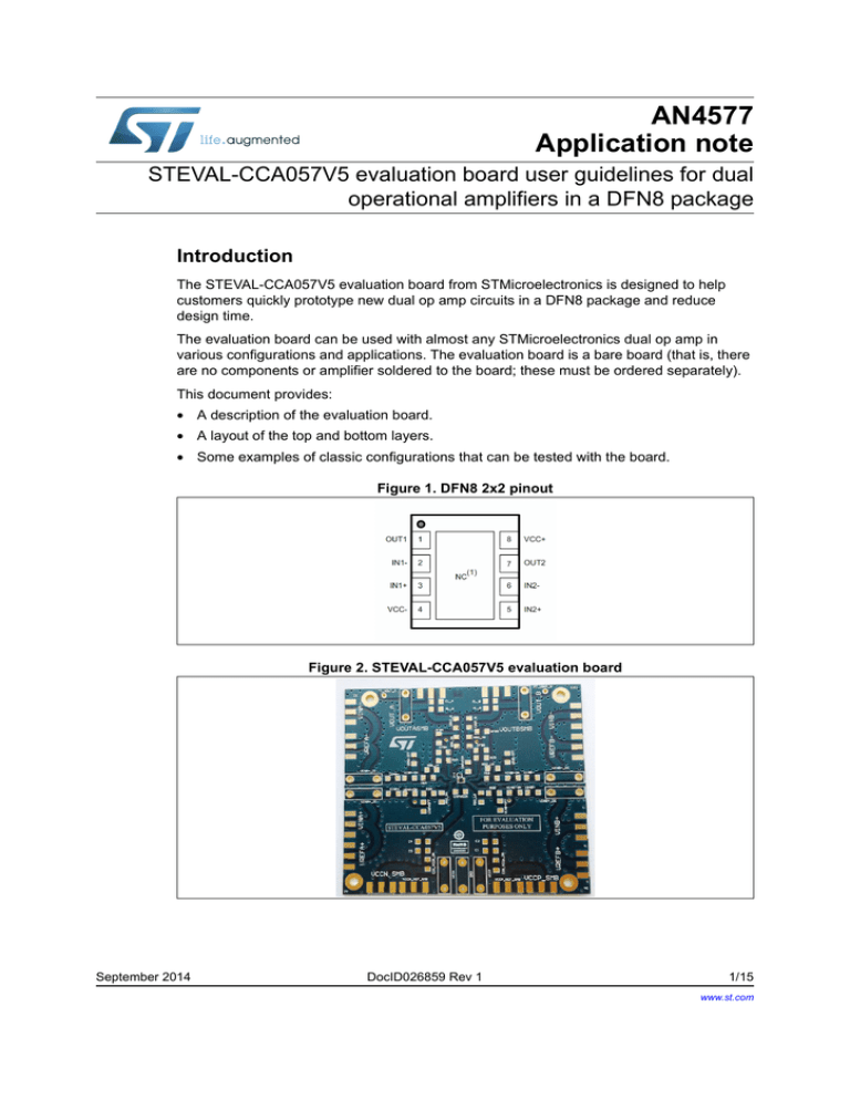
The STEVAL-CCA057V5 evaluation board from STMicroelectronics is designed to help
customers quickly prototype new dual op amp circuits in a DFN8 package and reduce
design time.
The evaluation board can be used with almost any STMicroelectronics dual op amp in
various configurations and applications. The evaluation board is a bare board (that is, there
are no components or amplifier soldered to the board; these must be ordered separately).
This document provides:
• A description of the evaluation board.
• A layout of the top and bottom layers.
• Some examples of classic configurations that can be tested with the board.
Figure 1. DFN8 2x2 pinout
Figure 2. STEVAL-CCA057V5 evaluation board
September 2014
DocID026859 Rev 1
1/15
www.st.com
15
Contents
AN4577
Contents
1
Description . . . . . . . . . . . . . . . . . . . . . . . . . . . . . . . . . . . . . . . . . . . . . . . . . 3
2
Layout . . . . . . . . . . . . . . . . . . . . . . . . . . . . . . . . . . . . . . . . . . . . . . . . . . . . . 6
3
Different possible configurations . . . . . . . . . . . . . . . . . . . . . . . . . . . . . . 7
3.1
Low-pass Sallen-key configuration . . . . . . . . . . . . . . . . . . . . . . . . . . . . . . . 7
3.2
High-pass Sallen-key configuration . . . . . . . . . . . . . . . . . . . . . . . . . . . . . . 8
3.3
Instrumentation amplifier . . . . . . . . . . . . . . . . . . . . . . . . . . . . . . . . . . . . . . 9
3.4
Transimpedance configuration . . . . . . . . . . . . . . . . . . . . . . . . . . . . . . . . . 10
3.5
AC coupled circuit configuration . . . . . . . . . . . . . . . . . . . . . . . . . . . . . . . . .11
4
Associated products . . . . . . . . . . . . . . . . . . . . . . . . . . . . . . . . . . . . . . . . 13
5
Revision history . . . . . . . . . . . . . . . . . . . . . . . . . . . . . . . . . . . . . . . . . . . 14
2/15
DocID026859 Rev 1
AN4577
1
Description
Description
This board is designed with versatility in mind, and allows many circuits to be constructed
easily and quickly.
A few possible circuits are as follows:
•
Voltage follower
•
Non-inverting amplifier
•
Inverting amplifier
•
Sallen-key filter
•
Instrument amplifier
•
AC-coupled circuit
•
Out-of-loop compensation circuit
Circuit
The circuit schematic in Figure 3 shows the connections for all possible components. Each
configuration uses only some of the components.
The board is designed for surface-mounted components and can be used to perform on
board characterization prior to the integration of STMicroelectronics products in your
designs. Resistor and capacitor footprints are implemented for the 1206 series.
DocID026859 Rev 1
3/15
15
VINB+
GND
VINB-
GND
VINA+
GND
VINA-
GND
2mm
0_CIN
CINA+
VREFA+
VINA-_DC
0_CIN
CINA-
VREFA-
VINB+_DC
0_CIN
CINB+
VREFB+
VINB-_DC
0_CIN
VREFBCINB-
VINA+_DC
2mm
2mm
DocID026859 Rev 1
2mm
VINB+ON
VINB-ON
VINA+ON
VINA-ON
GND
VINB+OFF
R1_0
GND
VINB-OFF
R1_0
GND
VINA+OFF
R1_0
GND
VINA-OFF
R1_0
R3_0
R3B
R1_0
R1B
R3_0
R3A
R1_0
R1A
GND
R50_2B
R4
R50_1B
50
GND
GND
R50_2A
R4
R50_1A
50
GND
5
VB- 6
GND
VB+
VCCP
V+
V-
7 VoutB
RFilterB
AOP-8PINS
IC1B
R2_0
CFB_OPEN
R2B
CFBB
RFilterA
1 VoutA
IC1A
AOP-8PINS
VCCN
CAPVCCP
3
VA- 2
VA+
R2_0
CFB_OPEN
R2A
CAPVCCN
GND
CFBA
4
4/15
8
0_50
R50_3B
RFBB
0_50
R50_3A
RFBA
COUT_A
0_COUT_RISO
COUT_B
0_COUT_RISO
GND
RL_B
RL_OPEN
GND
RL_A
RL_OPEN
CL_B
CL_OPEN
CL_A
CL_OPEN
GND
VOUTBSMB
2mm
VOUT_B
PT_VOUT_B
GND
VOUTASMB
2mm
VOUT_A
PT_VOUT_A
GND
GND
GND
GND
VCCN_REF_SMB
VCCN_SMB CIN_VCCN_ON
VCCN
2mm
VCCN
0_OPEN
C3
C4
GND
VCCP_REF_SMB
2mm
GND
VCCP_SMB CIN_VCCp_ON
VCCP
2mm
VCCP
0_COUT_RISO C1
C2
Description
AN4577
Figure 3. Evaluation board schematics
GSPG10092014DI1005
Power requirements
A 0Ω resistance must be connecting on CIN_VCCN_ON and CIN_VCCP_ON in order to
power supply the dual amplifier.
A set of two decoupling capacitors (C1, C2 and C3, C4) have been implemented on both
power supply pins, as to benefit from the maximum performances of ST products. In order
to reject low frequencies, 1 µF and 10 µF are good values for these.
AN4577
Description
Others decoupling capacitors (CAPVCCN, CAPVCCP) as close as possible of the MSO10
package, might also be used to obtain an excellent power supply decoupling. 100pF values
can be used in order to reject high frequencies.
When using single-supply circuits, the negative supply is shorted to ground by bridging C3
or C4 capacitances. Power is therefore between VCCP and GND.
Output options
The outputs have additional resistors (RL_A, RL_B) and capacitors (CL_A, CL_B)
placements for loading. Or it might be used as an anti-alias filter, or to limit amplifier output
noise by reducing its output bandwidth.
Note:
Operational amplifiers are sensitive to output capacitance and may oscillate. In event of
oscillation, reduce output capacitance by using shorter cables, or add a resistor in series on
COUT_A, COUT_B placement with a suitable value in order to improve amplifier phase
margin.
Measurement tips
In the datasheet, some measurements, as settling time, peaking, have been done with 50 Ω
output equipment. In order to keep the integrity of the square input signal, the input tracks
from VINA+, VINB+, VINA-, VINB+, have an impedance of 50 Ω.
And in order to adapt input impedance, 50 Ω resistances can be add on the R50_1A,
R50_2A and R50_1B, R50_2B.
DocID026859 Rev 1
5/15
15
Layout
2
AN4577
Layout
The board has the following physical characteristics.
•
Board dimensions: 3526 x 3300 mils (89.6 x 83.8 mm)
•
2-layer PCB
•
Both sides have a ground plane.
For Vout_A, Vout_B, VinA+,VinA-,VinB+ and VinB- female SMB or female 2 mm connectors
can be implanted. You can also implant test points on these voltages. They will facilitate the
visualization of your signals.
Top and bottom layers are shown on Figure 4 and Figure 5:
Figure 4. Top layer
6/15
Figure 5. Bottom layer
DocID026859 Rev 1
AN4577
3
Different possible configurations
Different possible configurations
The following provides some instructions on how to set up the board in order to perform
several classical configurations.
•
Figure 6: Low-pass Sallen-key 4th order configuration
•
Figure 7: High-pass Sallen-key configuration
•
Figure 8: Instrumentation amplifier
•
Figure 9: Transimpedance configuration
•
Figure 10: AC coupled circuit configuration
You can also put several boards in cascade which allows you to obtain a more complex
configuration.
3.1
Low-pass Sallen-key configuration
The following low-pass Sallen-key configuration is a fourth order filter configuration. This
circuit has 80dB roll-off per decade.
The transfer function is:
Equation 1
Equation 2
DocID026859 Rev 1
7/15
15
Different possible configurations
AN4577
Figure 6. Low-pass Sallen-key 4th order configuration
GND
RFA
CAPVCCN
GND
PT_VOUT_A
VCCN
VREFARGA
VA+
VINA-_DC
3
V+
2mm
0 ohms
VOUT_A
VOUTASMB
0 ohm
VCCP
R2
VREFA+
GND
1
VoutA
V-
8
VINA-
2mm
VA- 2
IC1A
AOP-8PINS
4
GND
GND
GND
C1
CAPVCCP
VINA+
2mm
GND
0 ohm
R1
GND
GND
VINA+_DC
GND
C2
RFB
GND
PT_VOUT_B
VREFB-
GND
RGB
2mm
VINB-
VB+
VINB-_DC
2mm VOUT_B
IC1B
VB- 6
7
VoutB
5
0 ohm
VOUTBSMB
0 ohm
AOP-8PINS
R4
VREFB+
GND
GND
GND
VINB+
2mm
C3
0 ohm
R3
GND
GND
VINB+_DC
GND
3.2
C4
GSPG10092014DI1010
High-pass Sallen-key configuration
Like the low-pass Sallen-key configuration above, this one is a fourth order. It has a slope of
+80dB per decade.
The transfer function is:
Equation 3
Equation 4
8/15
DocID026859 Rev 1
AN4577
Different possible configurations
Figure 7. High-pass Sallen-key configuration
GND
RFA
CAPVCCN
GND
PT_VOUT_A
VCCN
VREFARGA
VA+
VINA-_DC
3
V+
2mm VOUT_A
0 ohms
VOUTASMB
0 ohm
VCCP
C2
VREFA+
GND
1
VoutA
V-
8
VINA-
2mm
VA- 2
IC1A
AOP-8PINS
4
GND
GND
R1
GND
CAPVCCP
VINA+
2mm
GND
0 ohm
C1
GND
GND
VINA+_DC
GND
R2
RFB
GND
PT_VOUT_B
VREFB-
GND
2mm
VB- 6
VINB-
VB+
VINB-_DC
2mm
IC1B
RGB
7
VoutB
5
0 ohm
VOUTBSMB
0 ohm
AOP-8PINS
C4
VREFB+
GND
VOUT_B
GND
R3
GND
VINB+
2mm
GND
0 ohm
C3
GND
VINB+_DC
R4
GSPG0809141145SG
GND
The upper limit of the frequency range is determined by the GBP of the Opamp
3.3
Instrumentation amplifier
The instrumentation amplifier are generally used for precise measurement in a differential
way.
The architecture of Instrumentation amplifier with dual opamps is the simplest one. The
input impedance is high as the non-inverting of the both opamps are used as input.
By considering R1.R2=RFA.RFB
And Vout=Vreference for Vdiff =0V
The gain can be expressed as follow:
DocID026859 Rev 1
9/15
15
Different possible configurations
AN4577
Equation 5
Figure 8. Instrumentation amplifier
Rg
GND
RFA
CAPVCCN
GND
PT_VOUT_A
VCCN
VREFA-
Reference
0 ohms
0 ohms
R1
VA+
VINA-_DC
3
V+
VREFA+
GND
2mm
R2
VOUT_A
VOUTASMB
0 ohm
VCCP
0 ohm
GND
GND
CAPVCCP
GND
VINA+
2mm
Inverting
Input
1
VoutA
V-
8
2mm
VA- 2
VINA-
IC1A
AOP-8PINS
4
GND
0 ohm
0 ohm
GND
GND
VINA+_DC
GND
RFB
GND
PT_VOUT_B
VREFB-
GND
2mm
VB- 6
VINB-
2mm VOUT_B
IC1B
0 ohms
0 ohms
0 ohms
VINB-_DC
VB+
7
VoutB
5
VOUTBSMB
0 ohm
0 ohm
AOP-8PINS
Output
0 ohm
VREFB+
GND
GND
GND
GND
VINB+
2mm
Non
Inverting
Input
0 ohm
0 ohm
GND
VINB+_DC
GND
GSPG10092014DI1020
3.4
Transimpedance configuration
The Figure 9 shows how to configure op-amp IC1A as a transimpedance amplifier (TIA).
The output voltage of the TIA is the input current multiplied by the feedback resistor RFA:
Equation 6
VOUTA=(Iin+Ibias)*RFA-Vos
where Iin is defined as the input current source applied at the VINA- pad, IBIAS is the input
bias current, and VOS is the input offset voltage of the op amp. For the type of usage, the
feedback resistor RFA is generally high and the impedance seen on the VA- node is pretty
capacitive (ex: photodiode).In order to stabilize the Opamp it is recommended to connect a
feedback capacitance CF.
10/15
DocID026859 Rev 1
AN4577
Different possible configurations
Figure 9. Transimpedance configuration
Cf
GND
RFA
CAPVCCN
GND
PT_VOUT_A
VCCN
VREFA-
0 ohms
0 ohms
VA+
VINA-_DC
3
1
VoutA
VV+
2mm
0 ohm
8
VINA-
2mm
VA- 2
0 ohms
IC1A
AOP-8PINS
4
GND
VOUT_A
VOUTASMB
0 ohm
VCCP
VREFA+
GND
GND
GND
0 ohm
CAPVCCP
GND
GND
2mm
VINA+
GND
VINA+_DC
GND
0 ohm
GND
PT_VOUT_B
VREFB-
GND
2mm
VINB-
2mm VOUT_B
IC1B
VB- 6
5
0 ohm
VOUTBSMB
0 ohm
AOP-8PINS
VREFB+
GND
VB+
VINB-_DC
7
VoutB
GND
GND
0 ohm
GND
GND
2mm
VINB+
VINB+_DC
GSPG10092014DI1025
GND
Note:
If only IC1A opamp is used as transimpedance amplifier, the second one IC1B should be
configure in follower mode in order to avoid any undesired oscillation on its output.
3.5
AC coupled circuit configuration
This typical configuration allows you to amplify the AC part only of the input signal. As for
example typical stereo audio amplifier.
DocID026859 Rev 1
11/15
15
Different possible configurations
AN4577
Figure 10. AC coupled circuit configuration
GND
RFA
CAPVCCN
GND
PT_VOUT_A
VCCN
VREFA-
0 ohms
VINA-_DC
RGA-
CinA-
VA+
3
V+
2mm
0 ohm
CoutA
GND
R2
GND
VOUT_A
VOUTASMB
Rout
VCCP
RGA+
VREFA+
GND
1
VoutA
V-
8
VINA-
2mm
VA- 2
IC1A
AOP-8PINS
4
GND
CAPVCCP
VINA+
2mm
GND
0 ohms
CinA+
GND
GND
VINA+_DC
GND
RFB
GND
PT_VOUT_B
VREFB-
GND
2mm
VINB-
2mm VOUT_B
IC1B
VB- 6
0 ohms
VINB-_DC
RGB-
CinB-
VB+
5
7
VoutB
VOUTBSMB
RoutB
CoutB
RGB+
VREFB+
GND
0 ohm
AOP-8PINS
GND
GND
R3
VINB+
2mm
GND
0 ohms
CinB+
GND
VINB+_DC
GSPG0809141440SG
GND
12/15
DocID026859 Rev 1
AN4577
4
Associated products
Associated products
Table 1. Associated products
Part number
General description
LM258IQ2T
Low-power dual op-amps with low input bias current
LM2904IQ2T
Low power, bipolar op-amp
LM358IQ2T
Low-power dual op-amps with low input bias current
LMV822IQ2T
Low power, high accuracy, general purpose operational amplifier
LMX358IQ2T
Low-power, general-purpose operational amplifier
TSV522IQ2T
High merit factor (1.15 MHz for 45 uA) CMOS op-amps
TSV522AIQ2T
High merit factor (1.15 MHz for 45 uA) CMOS op-amps
TSV630IQ2T
Micro-power CMOS op-amp with standby
TSV632IQ2T
Micro-power CMOS op-amp
TSV632AIQ2T
Micro-power CMOS op-amp
TSV852IQ2T
Low-power, high accuracy, general-purpose operational amplifier
TSV912IQ2T
Rail to rail input/output widebandwidth op-amps
TSV991IQ2T
Rail to rail input/output high merit factor op-amps
TSZ122IQ2T
Very high accuracy (5 µV) zero drift micropower 5 V
DocID026859 Rev 1
13/15
15
Revision history
5
AN4577
Revision history
Table 2. Document revision history
14/15
Date
Revision
15-Sep-2014
1
Changes
Initial release.
DocID026859 Rev 1
AN4577
IMPORTANT NOTICE – PLEASE READ CAREFULLY
STMicroelectronics NV and its subsidiaries (“ST”) reserve the right to make changes, corrections, enhancements, modifications, and
improvements to ST products and/or to this document at any time without notice. Purchasers should obtain the latest relevant information on
ST products before placing orders. ST products are sold pursuant to ST’s terms and conditions of sale in place at the time of order
acknowledgement.
Purchasers are solely responsible for the choice, selection, and use of ST products and ST assumes no liability for application assistance or
the design of Purchasers’ products.
No license, express or implied, to any intellectual property right is granted by ST herein.
Resale of ST products with provisions different from the information set forth herein shall void any warranty granted by ST for such product.
ST and the ST logo are trademarks of ST. All other product or service names are the property of their respective owners.
Information in this document supersedes and replaces information previously supplied in any prior versions of this document.
© 2014 STMicroelectronics – All rights reserved
DocID026859 Rev 1
15/15
15
