User Guide 004
lSL8272MEVAL2Z Evaluation Board User Guide
Description
Key Features
The ISL8272M is a 50A step-down DC/DC power supply
module with an integrated digital PWM controller, dual-phase
synchronous power switches, inductors and passives. Only
input, output capacitors and minimal passives are needed to
finish the design. 50A of continuous output current can be
delivered without a need of airflow or heatsink. The ISL8272M
uses ChargeMode™ control (ASCR) architecture, which
responds to a transient load within a single switching cycle.
• VIN range of 4.5V to 14V, VOUT adjustable from 0.6V to 5V
The ISL8272MEVAL2Z evaluation board has three ISL8272M
modules connected in a current sharing configuration to
deliver 150A continuous output current. This evaluation board
comes with placeholders for pin-strap resistor to adjust output
voltage, soft-start timing, input UVLO threshold, control loop
response, current sharing configurations, and device PMBus™
address. More configurations, such as Digital-DC™ (DDC) bus
configuration and fault limits can be easily programmed or
changed via PMBus compliant serial bus interface.
ZLUSBEVAL3Z (USB to PMBus adapter) is provided with this
evaluation kit, which connects the evaluation board to a PC to
activate the PMBus communication interface. The PMBus
command set is accessed by using the PowerNavigator™
evaluation software from a PC running Microsoft Windows.
• Programmable VOUT, VOUT droop, margining, input and
output UVP/OVP, IOUT limit, OTP/UTP, soft-start, sequencing,
and external synchronization
• Monitor: VIN, VOUT, IOUT, temperature, duty cycle, switching
frequency and faults
• ChargeMode™ control tunable with PMBus
• Output FETs for load transient response evaluation
• Mechanical switch for enable and power-good LED indicator
Specifications
This board has been configured for the following operating
conditions by default:
• VIN = 5V TO 12V
• VOUT = 1.2V
• IMAX = 150A
• fSW = 421kHz
• 3-module current sharing with 0.1mV/A VOUT droop
• Output ripple: <5mVP-P
References
• ASCR gain = 200, ASCR residual = 90
ISL8272M datasheet
• Soft-start delay = 5ms; soft-start ramp time = 4ms
Ordering Information
PART NUMBER
ISL8272MEVAL2Z
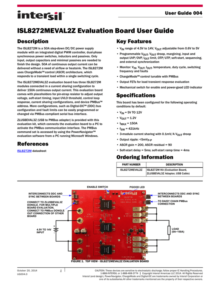
ENABLE SWITCH
DESCRIPTION
ISL8272M Kit (Evaluation Board,
ZLUSBEVAL3Z Adapter, USB Cable)
PGOOD LED
INTERCONNECTS DDC AND SYNC
BETWEEN BOARDS
INTERCONNECTS DDC AND
SYNC BETWEEN BOARDS
TO DAISY CHAIN PMBus
CONNECTION
CONNECT TO ZLUSBEVAL3Z
DONGLE. FOR MULTIPLE
BOARD EVALUATION,
CONNECT TO PMBus DONGLE
OUT CONNECTION OF OTHER
BOARD
+
4.5V TO 14V
INPUT
LOAD
(0A~150A)
-
FIGURE 1. TOP VIEW - lSL8272MEVAL2Z EVALUATION BOARD
October 20, 2014
UG004.0
1
CAUTION: These devices are sensitive to electrostatic discharge; follow proper IC Handling Procedures.
1-888-INTERSIL or 1-888-468-3774 | Copyright Intersil Americas LLC 2014. All Rights Reserved
Intersil (and design), PowerNavigator, ChargeMode and Digital-DC are trademarks owned by Intersil Corporation or
one of its subsidiaries.All other trademarks mentioned are the property of their respective owners.
User Guide 004
RESISTOR PLACEHOLDERS
FIGURE 2. BOTTOM VIEW - lSL8272MEVAL2Z EVALUATION BOARD
Recommended Equipment
• DC power supply with minimum 15V/40A sourcing capacity
• Electronic load capable of sinking current up to 150A
• Digital multimeters (DMMs)
• Oscilloscope with bandwidth higher than 100MHz
1. Set ENABLE switch to “DISABLE”.
2. Connect Load to VOUT lug connectors (J19, J21, J23 and J20,
J22, J25).
3. Connect power supply to VIN connectors (J9, J10 and J11,
J12). Make sure power supply is not enabled when making
connection.
4. Turn power supply on.
Functional Description
5. Set ENABLE switch to “ENABLE”.
The ISL8272MEVAL2Z provides all circuitry required to evaluate
the current sharing features of the ISL8272M. A majority of the
features of the ISL8272M, such as compensation-free
ChargeMode™ control, soft-start delay and ramp times and
voltage margining are available on this evaluation board. For
DDC communication evaluation, the board can be connected to
any Intersil digital module evaluation board that supports the
DDC bus.
7. Observe switching frequency of 421kHz and phase spreading
at probe points labeled “PHASE1_1” (TP7), “PHASE2_1”
(TP8), “PHASE1_2” (TP23), “PHASE2_2” (TP24), “PHASE1_3”
(TP15), “PHASE2_3” (TP16).
Figures 1 and 2 show the board images of the ISL8272MEVAL2Z
evaluation board.
Quick Start Guide
Pin-Strap Option
ISL8272MEVAL2Z can be configured in pin-strap mode with
standard 1% 0603 resistors. PMBus interface is not required to
evaluate ISL8272M in pin-strap mode. Output voltage (VOUT),
soft-start timing, input undervoltage protection (UVLO) threshold,
ASCR gain and residual, current sharing configuration and device
PMBus address can be changed by populating recommended
resistors at placeholders provided in the evaluation board. By
default, the evaluation board operates in pin-strap mode and
regulates at VOUT = 1.2V, fSW = 421kHz, soft-start delay
time = 5ms, soft-start ramp time = 4ms, UVLO = 4.5V, ASCR gain
= 200, ASCR residual = 90 and PMBus address = 2Ah, 2Bh, 2Ch.
In addition, the three modules are pin strapped for current
sharing, with a VOUT droop of 0.1mV/A. Follow these steps to
evaluate ISL8272M in pin-strap mode.
Submit Document Feedback
2
6. Measure 1.2V VOUT at probe point labeled “VOUT MONITOR”
(J24).
8. To measure the board efficiency, connect the multimeter
voltage probes at probe points labeled “VIN” (TP26), “GND”
(TP25) and “VOUT” (TP27), “GND” (TP28).
9. To change VOUT, disconnect board from the setup and
populate 1% standard 0603 resistors at R4, R34 and R19
placeholder locations on the bottom layer. Refer to the
“Output Voltage Resistor Settings” table in the ISL8272M
datasheet for recommended values. By default, VOUT_MAX is
set to 110% of VOUT set by pin-strap resistor. Keep in mind
that modules in the same current sharing group must have
identical VSET pin-strap resistors. For higher output voltage
setting, VOUT droop must be increased proportionally to
ensure good current sharing.
10. To change soft-start delay and ramp time, disconnect board
from the setup and populate 1% standard 0603 resistors at
R6, R36 and R21 placeholder locations on the bottom layer.
Refer to the “Soft Start/Stop Resistor Settings” table in the
ISL8272M datasheet for recommended values. Notice that
only immediate off is supported in current sharing
configuration.
11. To change UVLO, disconnect board from the setup and
populate standard 0603 resistors at R6, R36 and R21
UG004.0
October 20, 2014
User Guide 004
placeholder locations on the bottom layer. Refer to the “UVLO
Resistor Settings” table in the ISL8272M datasheet for
recommended values. Notice that the UVLO programming
shares the same pin with soft-start/stop programming.
12. To change ASCR gain and residual, disconnect board from the
setup and populate 1% standard 0603 resistors at R8, R38
and R23 placeholder locations on the bottom layer. Refer to the
“ASCR Resistor Settings” table and the design guide matrix in
the ISL8272M datasheet for recommended values. Modules in
the same current sharing group must have identical ASCR gain
and residuals.
13. To change current sharing configuration, disconnect board
from the setup and replace with 1% standard 0603 resistors
at R5, R35 and R20 on the bottom layer. Refer to the “Current
Sharing Resistor Settings” table in the ISL8272M datasheet for
recommended values. For example, using 12.1k for R5, 13.3k
for R35 and OPEN for R20 will configure two modules for
current sharing (with a VOUT droop of 0.15mV/A) and the third
module as stand alone.
PMBus Option
ISL8272MEVAL2Z can be evaluated for all features particularly in
the current sharing configuration using the provided
ZLUSBEVAL3Z dongle and PowerNavigator™ evaluation software.
Follow these steps to evaluate ISL8272M with PMBus option.
1. Install the PowerNavigator™ evaluation software from the
following Intersil website: www.intersil.com/powernavigator
2. Set ENABLE switch to “DISABLE”.
3. Connect Load to VOUT lug connectors (J19, J21, J23 and J20,
J22, J25).
4. Connect power supply to VIN connectors (J9, J10 and J11,
J12). Make sure power supply is not enabled when making
connection.
5. Turn power supply on.
6. Connect ZLUSBEVAL3Z dongle (USB to PMBus™ adapter) to
ISL8272MEVAL2Z board to the 6-pin male connector labeled
as “PMBus DONGLE IN”.
7. Connect supplied USB cable from computer USB to
ZLUSBEVAL3Z dongle.
settings, disable the module and use the command
RESTORE_FACTORY and STORE_USER_ALL.
12. PowerNavigator™ tutorial videos are available at Intersil
website. www.intersil.com/powernavigator
13. To evaluate multiple Intersil digital power products using a
single ZLUSBEVAL3Z dongle, ISL8272M can be daisy chained
with other digital power evaluation boards. PMBus address
can be changed by replacing with 1% standard 0603 resistors
at R3, R33 and R18 locations on the bottom layer. Refer to
the “SMBus Address Resistor Selection” table in the
ISL8272M datasheet for recommended values.
Evaluation Board Information
The evaluation board size is 5.8in x 6.1in. It is a 6-layer board,
containing 2-ounce copper on all layers. The board can be used
as a 150A reference design. Refer to the “ISL8272MEVAL2Z
Evaluation Board Layout” beginning on page 13. The board is
made of FR4 material and all components, including the solder
attachment, are lead-free.
VOUT Transient Response Measurement
The ISL8272MEVAL2Z board has a built-in transient load test
circuitry (see the schematic in Figure 3). Two 100A N-Channel
MOSFETs (Manufacturer PN: BSC010NE2LS) are connected in
parallel across VOUT and PGND next to the remote voltage
sensing location (C98). Two 10mΩ current sense resistors
connected in parallel are placed for monitoring the
drain-to-source current of the MOSFETs. For a transient load test,
inject the gate driver pulse signal at J16, which is labeled as
“TRANSIENT LOAD INPUT.” The load current can be monitored
through J15, which is labeled as “TRANSIENT LOAD MONITOR.”
Because the two MOSFETs will operate in the saturation region
instead of linear region when the gate turn-on signal is applied,
the pulse width and duty cycle of the gate signal must be
sufficiently small to avoid MOSFETs overheating (recommended
duty cycle should be less than 2% to 3%). The amplitude of the
gate driver pulse voltage can be adjusted to obtain a desired
transient load current step size.
VOUT
VOUT
8. Launch PowerNavigator™ software.
9. It is optional to load a predefined setup from three separate
configuration files using the PowerNavigator™ software. The
three ISL8272M devices on the board operate in pin-strap
mode from factory default, but the user may modify the
operating parameters through the evaluation software or by
loading a predefined setup from configuration files. A sample
set of the “Configuration File” beginning on page 11 is
provided and can be copied to a notepad editor to make
desired changes. The default pin-strap configurations will be
overwritten if user-defined configuration files are loaded.
10. Set ENABLE switch to “ENABLE”. Alternately, the PMBus
commands ON_OFF_CONFIG and OPERATION may be used
from the PowerNavigator™ software to allow PMBus Enable.
2 X BSC010NE2LS
2 x BSC010NE2LS
+
‐
+
‐
J16
J16
J15
J15
2 x 10mє
2 x 10mΩ Ŝ
TRANSIENT LOAD TRANSIENT LOAD
ULSE
INPUT
PULSE INPUT
TRANSIENT TRANSIENT
LOAD MONITOR
LOAD MONITOR
FIGURE 3. SCHEMATIC FOR TRANSIENT LOAD MEASUREMENT
11. Monitor and configure the ISL8272MEVAL2Z board using the
PMBus commands in the evaluation software. To store the
configuration changes, disable the module and use the
command STORE_USER_ALL. To restore factory default
Submit Document Feedback
3
UG004.0
October 20, 2014
User Guide 004
Control Loop Bode Plot Measurement
To measure the bode plot of the voltage control loop, the first
step is to break the loop such that a small signal with variable
frequency can be injected at a certain point. On this
ISL8272MEVAL2Z evaluation board, the 0Ω resistor R58 placed
in the VOUT remote sense line can be replaced by a 5Ω ~10Ω
resistor. The placeholders J17 and J18 can be used to inject the
frequency-sweep signal across R58 from a network analyzer.
Connect the network analyzer input (Channel A) at J17 and
output (Channel B) at J18 to measure the voltage loop transfer
function and frequency responses. See the configuration
diagram in Figure 4.
VOUT
VOUT
Network NETWORK
ANALYZER
Analyzer
ISL8272M
ISL8272M
VSENP
VSENP
AA
B
TO
To LOAD
Load
VOUT
VOUT
ISL8272M
ISL8272M
R58
R58
VSENP
VSENP
VOUT
VOUT
J17
J17
+
+
-‐
10Ω
10 Ohm
++
-‐
J18
J18
ISL8272M
ISL8272M
VSENP
VSENP
SIGNAL
GENERATOR
Signal Generator
FIGURE 4. CONFIGURATION FOR VOLTAGE LOOP BODE PLOT
MEASUREMENT
power planes in different layers under and around the
modules.
2. SW1 and SW2 pads are switching nodes that generate
switching noises. Keep these pads under the module. For
noise-sensitive applications, it is recommended to keep
switching node pads only on the top and inner layers of the
PCB; do not place switching node pads exposed to the outside
on the bottom layer of the PCB. To improve the thermal
performance, the switching node pads can be extended in the
inner layer (Layer 3 on this board), as shown on the
“ISL8272MEVAL2Z Evaluation Board Layout” beginning on
page 13. Make sure that Layer 2 and Layer 4 have the GND
planes to cover the extended areas of the switching node
pads at Layer 3 to avoid noise coupling.
3. To create a low impedance path for the high frequency
inductor ripple current, output ceramic capacitors must be
placed very close to the center of the module VOUT pads.
Therefore, multiple vias must be applied to ground these
ceramic capacitors to the PGND planes in the inner layers.
Make sure these vias can sufficiently handle the inductor
ripple current.
4. Place the modules evenly on the board and leave enough
space between modules. If the board space is limited, try to
put the modules with low power loss closly (e.g., low VOUT or
IOUT) while still separating the module with high power loss.
5. If the ambient temperature is high or the board space is
limited, airflow is needed to dissipate more heat from the
modules. A heatsink can also be applied to the top side of the
module to further improve the thermal performance.
Thermal Considerations and Current Derating
Board layout is very critical in order to make the module operate
safely and deliver maximum allowable power. To work in the high
temperature environments and carry large currents, the board
layout needs to be carefully designed to maximize thermal
performance. To achieve this, select enough trace width, copper
weight and the proper connectors.
The ISL8272MEVAL2Z evaluation board is designed for running
150A at room temperature under default configurations without
additional cooling. However, if the output voltage is increased or
the board is operated at elevated temperatures, then the
available output current is derated. Typically, the module
temperatures is higher on the current sharing board compared to
the single-module board under the same operating conditions
due to the limited PCB copper planes for heat sink. For
single-module operation, refer to the derated current curves in
the ISL8272M datasheet to determine the maximum output
current the module can supply. JA is measured by inserting a
thermocouple inside the module to measure peak junction
temperature.
For layout of current sharing designs using the ISL8272M, the
thermal performance can be improved by adhering to the
following design tips:
1. Use the top and bottom layers to carry the large current. One
or more inner layers can also be used to carry the large
current if available. VOUT, PGND and VIN pads should have
large, solid planes. Place enough thermal vias to connect the
Submit Document Feedback
4
UG004.0
October 20, 2014
VR55_1
C8
C10
10UF
TP6
TP2
10UF
Submit Document Feedback
ISL8272MEVAL2Z Schematics
E14
D14
EN
NC
PGND
PGND
PGND
PGND
PGND
C23
OPEN
C22
OPEN
C21
100UF
C20
100UF
C19
OPEN
C18
OPEN
C17
100UF
C16
100UF
C12
VSENN
PHASE2_1
TP8
PG1_1
UNNAMED_1_SMRES_I228_B
R8
PAD10
PAD12
M5
M17
N5
VOUT
OPEN
PAD1
PAD3
PAD5
L3
PAD14
PAD13
H4
H3
PAD2
PAD4
PAD7
P11
PAD16
PAD15
E15
F15
D5
G14
DNP
VDRV1
VDRV1
R8
R17
L2
M10
K14
VDD
VR
VR55
VIN
VIN
VIN
N6
N16
M1
G15
L14
M13
R6
U1
UNNAMED_1_SMRES_I205_B
DNP
R5
UNNAMED_1_SMRES_I240_B
34.8K
R4
R3
51.1K
UNNAMED_1_SMRES_I204_B
DNP
R2
6.65K
UNNAMED_1_SMRES_I37_B
VSENP
VOUT
PGND
PGND
SWD1
SW1
PGND
VSENP
VSENN
VOUT
PGND
PGND
SWD2
SW2
PGND
NC
NC
PG
ASCR
ISL8272MIRZ
VDRV
VDRV
VCC
V25
VR5
VR6
R1
100K
MGN
SCL
SDA
SALRT
SA
DDC
SYNC
NC
NC
VSET
NC
MGN
CS
SS/UVLO
VMON
SGND
SGND
SGND
SGND
SGND
TP7
User Guide 004
C13
C12
C11
C10
E4
D13
F4
G4
C6
C5
C8
C7
D4
C9
H16
J16
K16
M14
PAD6
DDC
SYNC
UNNAMED_1_SMRES_I39_B
EN
DNP
SCL
SDA
SALRT
VCC_1
J3
1 2
PHASE1_1
PAD8
PAD9
PAD11
C5
22UF
C4
22UF
C3
22UF
C2
22UF
C1
150UF
5
VCC_1
VIN
DNP
J4
TP3
VR6_1
C11
10UF
10UF
TP1
VR5_1
V25_1
VCC_1
C9
C7
10UF
C6
10UF
1 2
TP4
DRAWN BY:
TP5
GND_POWER TIED TO GND
UNDER DUT
TIM KLEMANN
ENGINEER:
DATE:
DATE:
UPDATED BY:
DATE:
DATE:
EVAN JIANG
09/15/2014
RELEASED BY:
TITLE:
ISL8272M 3X50A
EVALUATION BOARD
SCHEMATIC
TESTER
$CDS_IMAGE|intersil_color_sm.jpg|1194|282
MASK#
HRDWR ID
ISL8272MEVAL2Z
REV.
C
UG004.0
October 20, 2014
VR55_2
TP22
C56
10UF
TP18
C54
10UF
Submit Document Feedback
ISL8272MEVAL2Z Schematics (Continued)
J7
EN
VCC_2
C51
22UF
C50
22UF
C49
22UF
22UF
C47
6
C48
150UF
VIN
1 2
DNP
E14
D14
EN
NC
C69
OPEN
C68
OPEN
C67
100UF
C66
100UF
C65
OPEN
C64
OPEN
C63
100UF
C62
100UF
C58
VSENN
PHASE2_2
TP24
PG1_2
UNNAMED_3_SMRES_I58_B
R38
N6
N16
M1
G15
L14
M13
VOUT
OPEN
L2
M10
R8
R17
VDRV1
VDRV1
K14
VDD
VIN
VIN
VIN
U2
UNNAMED_3_SMRES_I48_B
DNP
R36
UNNAMED_3_SMRES_I104_B
38.3K
UNNAMED_3_SMRES_I45_B
R35
R34
R33
56.2K
UNNAMED_3_SMRES_I34_B
DNP
R32
6.65K
UNNAMED_3_SMRES_I40_B
PAD1
PAD3
PAD5
L3
PAD14
PAD13
H4
H3
PAD2
PAD4
PAD7
P11
PAD16
PAD15
E15
F15
D5
G14
DNP
MGN
ISL8272MIRZ
PAD10
PAD12
M5
M17
N5
R31
100K
VCC_2
VSENP
VOUT
PGND
PGND
SWD1
SW1
PGND
VSENP
VSENN
VOUT
PGND
PGND
SWD2
SW2
PGND
NC
NC
PG
ASCR
PGND
PGND
PGND
PGND
PGND
DDC
SYNC
SCL
SDA
SALRT
SA
DDC
SYNC
NC
NC
VSET
NC
MGN
CS
SS/UVLO
VMON
SGND
SGND
SGND
SGND
SGND
TP23
User Guide 004
C13
C12
C11
C10
E4
D13
F4
G4
C6
C5
C8
C7
D4
C9
H16
J16
K16
M14
PAD6
VDRV
VDRV
VCC
V25
VR5
VR6
SCL
SDA
SALRT
VR
VR55
PAD8
PAD9
PAD11
PHASE1_2
J8
1 2
TP19
VR5_2
TP20
10UF
C57
VR6_2
10UF
TP17
V25_2
VCC_2
C55
C53
10UF
C52
10UF
DNP
TP21
DRAWN BY:
GND_POWER TIED TO GND
TIM KLEMANN
DATE:
ENGINEER:
RELEASED BY:
DATE:
UPDATED BY:
DATE:
DATE:
EVAN JIANG
09/15/2014
TITLE:
ISL8272M 3X50A
UNDER DUT
EVALUATION BOARD
SCHEMATIC
TESTER
$CDS_IMAGE|intersil_color_sm.jpg|1194|282
MASK#
HRDWR ID
ISL8272MEVAL2Z
REV.
C
UG004.0
October 20, 2014
VR55_3
TP14
C33
10UF
TP10
C31
10UF
Submit Document Feedback
ISL8272MEVAL2Z Schematics (Continued)
C28
22UF
C27
22UF
C26
22UF
C25
22UF
C24
150UF
J5
EN
7
VCC_3
VIN
1 2
DNP
E14
D14
EN
NC
U3
C46
OPEN
C45
OPEN
C44
100UF
C43
100UF
C42
OPEN
C41
OPEN
C40
100UF
C39
100UF
C35
VSENN
PHASE2_3
TP16
PG1_3
UNNAMED_2_SMRES_I77_B
R23
PAD10
PAD12
M5
M17
N5
N6
N16
M1
G15
L14
M13
VOUT
OPEN
R8
R17
VDRV1
VDRV1
L2
M10
K14
VDD
VIN
VIN
VIN
ISL8272MIRZ
UNNAMED_2_SMRES_I62_B
DNP
R21
UNNAMED_2_SMRES_I115_B
42.2K
UNNAMED_2_SMRES_I59_B
R20
R19
61.9K
R18
UNNAMED_2_SMRES_I55_B
DNP
R17
6.65K
UNNAMED_2_SMRES_I57_B
VOUT
PGND
PGND
SWD1
SW1
PGND
VSENP
VSENN
VOUT
PGND
PGND
SWD2
SW2
PGND
NC
NC
PG
ASCR
DNP
100K
MGN
VSENP
PAD1
PAD3
PAD5
L3
PAD14
PAD13
H4
H3
PAD2
PAD4
PAD7
P11
PAD16
PAD15
E15
F15
D5
G14
User Guide 004
R16
VCC_3
SCL
SDA
SALRT
SA
DDC
SYNC
NC
NC
VSET
NC
MGN
CS
SS/UVLO
VMON
SGND
SGND
SGND
SGND
SGND
TP15
PGND
PGND
PGND
PGND
PGND
DDC
SYNC
C13
C12
C11
C10
E4
D13
F4
G4
C6
C5
C8
C7
D4
C9
H16
J16
K16
M14
PAD6
VDRV
VDRV
VCC
V25
VR5
VR6
SCL
SDA
SALRT
VR
VR55
PAD8
PAD9
PAD11
PHASE1_3
J6
1 2
TP11
TP12
10UF
VR6_3
C34
10UF
TP9
VR5_3
V25_3
VCC_3
C32
C30
10UF
C29
10UF
DNP
TP13
DRAWN BY:
GND_POWER TIED TO GND
UNDER DUT
TIM KLEMANN
DATE:
ENGINEER:
RELEASED BY:
DATE:
UPDATED BY:
DATE:
DATE:
EVAN JIANG
09/15/2014
TITLE:
ISL8272M 3X50A
EVALUATION BOARD
SCHEMATIC
TESTER
$CDS_IMAGE|intersil_color_sm.jpg|1194|282
MASK#
HRDWR ID
REV.
UG004.0
October 20, 2014
SYNC
2
1
INTER-DEVICE COMM
R64
4.75K
R62
4.75K
R61
4.75K
R60
4.75K
C97
0.1UF
10K
C96
0.1UF
J13
1 2
FROM PREQUEL
PMBUS DONGLE COMM
J26
SYNC 1
FROM PREQUEL
2
EN
TRANSIENT LOAD MONITOR
MGN
SW1
0.01
R55
0.01
R54
J14
8
J15
U4
1 2
1
1 2
3
UNNAMED_5_GTSERIES_I39_NC
1
DP
2
4
47K
8
1
7
3
R57
SDA
SCL
VI2C
1
3
5
U5
UNNAMED_5_BSC010NE2LS5_I144_S1
6
UNNAMED_5_BSC010NE2LS5_I144_G
5
DP
8
2
7
3
6
4
5
3
5
J1
DDC
ENABLE
DISABLE
VCC_COM
D7
VCC_1
VCC_COM
VCC_COM
R46
Submit Document Feedback
ISL8272MEVAL2Z Schematics (Continued)
1 2
3 4
5 6
2
4
6
SALRT
SYNC
J27
1
3
5
J2
1 2
3 4
5 6
DDC
TO SEQUEL
EN
TO SEQUEL
1
3
5
2
4
6
1 2
3 4
5 6
2
4
6
1 2
3 4
5 6
DDC
2
4
6
1 2
J16
TRANSIENT LOAD INPUT
DNP
1 2
DNP
J18
1 2
J17
C92
470UF
C84
C77
470UF
C75
C74
470UF
VSENP
J21
J23
R58
TP27
VOUT MONITOR
C71
470UF
C70
VOUT
J19
0
VSENN
TP28
R52
VCC_2
R51
UNNAMED_5_SMRES_I96_B
1
2N7002L
2
D2
4
2
Q1
2
J24
1 2
J25
D3
1
3
D1
4
3
UNNAMED_5_NCHANNEL_I85_D
1
J22
GRN
RED
GRN
RED
GRN
RED
2
J20
UNNAMED_5_SMRES_I100_B
1.5K
3
PG1_1
UNNAMED_5_SMRES_I99_B
1.5K
R53
UNNAMED_5_SMRES_I98_B
1.5K
1
1.5K
VCC_3
3
R47
R56
UNNAMED_5_SMRES_I97_B
1.5K
200
0
3
UNNAMED_5_SMRES_I95_B
1.5K
4
R48
R63
R59
GND
VCC_1
22UF
C98
470UF
C86
470UF
C80
470UF
C88
470UF
C82
470UF
C94
470UF
C90
100UF
C83
C81
100UF
100UF
C79
100UF
C78
100UF
C73
TP25
GND
C76
J12
100UF
VOUT
J11
User Guide 004
470UF
470UF
VIN
470UF
C72
TP26
J10
470UF
VIN
J9
PG1_2
Q2
1
2
2N7002L
DRAWN BY:
3
UNNAMED_5_NCHANNEL_I79_D
UNNAMED_5_NCHANNEL_I45_D
PG1_3
TIM KLEMANN
DATE:
ENGINEER:
DATE:
UPDATED BY:
DATE:
TITLE:
Q3
1
2
2N7002L
ISL8272M 3X50A
EVALUATION BOARD
SCHEMATIC
TESTER
$CDS_IMAGE|intersil_color_sm.jpg|1194|282
DATE:
EVAN JIANG
09/15/2014
RELEASED BY:
MASK#
HRDWR ID
ISL8272MEVAL2Z
REV.
C
UG004.0
October 20, 2014
User Guide 004
Bill of Materials
REFERENCE DESIGNATORS
QTY
MANUFACTURER
MANUFACTURER PART
DESCRIPTION
C12, C35, C58
0
C96, C97
2
PANASONIC
ECJ-2VB1E104K
CAP, SMD, 0805, 0.1µF, 25V, 10%, X7R,
ROHS
C98
1
TDK
C2012X5R0J226M
CAP, SMD, 0805, 22µF, 6.3V, 20%, X5R,
ROHS
C6, C7, C9, C11, C29, C30, C32, C34,
C52, C53, C55, C57
12
VENKEL
C1206X7R100-106KNE
CAP, SMD, 1206, 10µF, 10V, 10%, X7R, ROHS
6
VENKEL
C1206X7R250-106KNE
CAP, SMD, 1206, 10µF, 25V, 10%, X7R, ROHS
C16, C17, C20, C21, C39, C40, C43,
C44, C62, C63, C66, C67, C73, C76,
C78, C79, C81, C83
18
MURATA
GRM31CR60J107ME39L
CAP, SMD, 1206, 100µF, 6.3V, 20%, X5R,
ROHS
C18, C19, C22, C23, C41, C42, C45,
C46, C64, C65, C68, C69
0
C2, C3, C4, C5, C25, C26, C27, C28,
C48, C49, C50, C51
12
MURATA
GRM32ER71C226KE18L
CAP, SMD, 1210, 22µF, 16V, 10%, X7R, ROHS
C1, C24, C47
3
SANYO/PANASONIC
16TQC150MYF
CAP-POSCAP, SMD, 7.3x4.3, 150µF, 16V,
20%, 50mΩ, ROHS
C72, C74, C77, C90, C92, C94
6
SANYO
6TPE470MI
CAP-POSCAP, LOW ESR, SMD, D4, 470µF,
6.3V, 20%, 18mΩ, ROHS
C70, C71
2
PANASONIC
EEE-1EA471P
CAP, SMD, 10mm, 470µF, 25V, 20%,
ALUM.ELEC., 380mA, ROHS
J9, J10, J11, J12
4
JOHNSON COMPONENTS 108-0740-001
CONN-JACK, BANANA-SS-SDRLESS,
VERTICAL, ROHS
TP7, TP8, TP15, TP16, TP23, TP24,
TP25-TP28
10
KEYSTONE
5005
CONN-COMPACT TEST PT, VERTICAL, RED,
ROHS
J13, J14, J15, J16, J24
5
BERG/FCI
69190-202HLF
CONN-HEADER, 1x2, RETENTIVE, 2.54mm,
0.230 x 0.120, ROHS"
J2, J27
2
SAMTEC
SSQ-103-02-T-D-RA
CONN-SOCKET STRIP, TH, 2x3, 2.54mm, TIN,
R/A, ROHS
J1, J26
2
SAMTEC
TSW-103-08-T-D-RA
CONN-HEADER, 2x3, BRKAWY, 2.54mm, TIN,
R/A, ROHS
D7
1
ON SEMICONDUCTOR
BAT54XV2T1G
DIODE-SCHOTTKY, SMD, 2P, SOD523, 30V,
200mA, ROHS
D1, D2, D3
3
LUMEX
SSL-LXA3025IGC-TR
LED, SMD, 3x2.5mm, 4P, RED/GREEN,
12/20MCD, 2V
U1, U2, U3
3
INTERSIL
ISL8272MAIRZ
IC-50A DIGITAL DC/DC MODULE, 42P, HDA,
ROHS
Q1, Q2, Q3
3
ON SEMICONDUCTOR
2N7002LT1G
TRANSISTOR-MOS, N-CHANNEL, SMD, SOT23,
60V, 115mA, ROHS
U4, U5
2
INFINEON TECHNOLOGY
BSC010NE2LS
TRANSIST-MOS, N-CHANNEL, 8P,
PG-TDSON-8, 25V, 100A, ROHS
C8, C10, C31, C33, C54, C56
Submit Document Feedback
9
CAP, SMD, 0603, DNP-PLACE HOLDER, ROHS
CAP, SMD, 1206, DNP-PLACE HOLDER, ROHS
UG004.0
October 20, 2014
User Guide 004
Bill of Materials (Continued)
REFERENCE DESIGNATORS
QTY
MANUFACTURER
MANUFACTURER PART
DESCRIPTION
R4, R6, R8, R19, R21, R23, R34,
R36, R38
0
R46
1
PANASONIC
ERJ-2RKF1002X
RES, SMD, 0402, 10k, 1/16W, 1%, TF, ROHS
R60, R61, R62, R64
4
PANASONIC
ERJ-2RKF4751X
RES, SMD, 0402, 4.75k, 1/16W, 1%, TF,
ROHS
R58, R59
2
VENKEL
CR0603-10W-000T
RES, SMD, 0603, 0Ω, 1/10W, TF, ROHS
R1, R16, R31
3
VENKEL
CR0603-10W-1003FT
RES, SMD, 0603, 100k, 1/10W, 1%, TF, ROHS
R47, R48, R51-R53, R56
6
VENKEL
CR0603-10W-1501FT
RES, SMD, 0603, 1.5k, 1/10W, 1%, TF, ROHS
R5
1
VENKEL
CR0603-10W-3482FT
RES, SMD, 0603, 34.8k, 1/10W, 1%, TF,
ROHS
R35
1
PANASONIC
ERJ-3EKF3832V
RES, SMD, 0603, 38.3k, 1/10W, 1%,TF, ROHS
R20
1
ROHM
TRR03EZPF4222
RES, SMD, 0603, 42.2k, 1/10W, 1%, TF,
ROHS
R57
1
YAGEO
RC0603FR-0747KL
RES, SMD, 0603, 47k, 1/10W, 1%, TF, ROHS
R3
1
VENKEL
CR0603-10W-5112FT
RES, SMD, 0603, 51.1k, 1/10W, 1%, TF,
ROHS
R33
1
VENKEL
CR0603-10W-5622FT
RES, SMD, 0603, 56.2k, 1/10W, 1%, TF,
ROHS
R18
1
PANASONIC
ERJ-3EKF6192V
RES, SMD, 0603, 61.9k, 1/10W, 1%, TF,
ROHS
R2, R17, R32
3
YAGEO
RC0603FR-076K65L
RES, SMD, 0603, 6.65k, 1/10W, 1%, TF,
ROHS
R63
1
PANASONIC
ERJ-6ENF2000V
RES, SMD, 0805, 200Ω, 1/8W, 1%, TF, ROHS
R54, R55
2
VISHAY/DALE
WSL2512R0100FEA
RES, SMD, 2512, 0.01Ω, 1W, 1%, TF, ROHS
SW1
1
C&K COMPONENTS
GT13MCBE
SWITCH-TOGGLE, THRU-HOLE, 5PIN, SPDT,
3POS, ON-OFF-ON, ROHS
J19, J20, J21, J22, J23, J25
6
BERG/FCI
KPA8CTP
HDWARE, MTG, CABLE TERMINAL, 6-14AWG,
LUG&SCREW, ROHS
C75, C80, C82, C84, C86, C88
0
CAP-POSCAP, DNP-PLACE HOLDER
J3, J4, J5, J6, J7, J8, J17, J18
0
CONN-HEADER, 1x2, 2.54mm, DNP-PLACE
HOLDER
TP1-TP6, TP9-TP14, TP17-TP22
0
CONN-COMPACT TEST PT, DNP-PLACE
HOLDER
Submit Document Feedback
10
RESISTOR, SMD, 0603, 0.1%, MF, DNP-PLACE
HOLDER
UG004.0
October 20, 2014
User Guide 004
Configuration File
Sample Configuration Files for ISL8272M Module Current Sharing. For each device, copy and
paste the corresponding lines (from RESTORE_FACTORY to ### End User Store) to a notepad and save it as
Confile_file_device_number.txt. The # symbol is used for a comment line. Some of the following settings are already loaded to
ISL8272M module as factory defaults.
# Device #1
RESTORE_FACTORY
STORE_USER_ALL
# VOUT Related
VOUT_COMMAND
VOUT_MAX
VOUT_MARGIN_HIGH
VOUT_MARGIN_LOW
VOUT_OV_FAULT_LIMIT
VOUT_OV_FAULT_RESPONSE
VOUT_OV_WARN_LIMIT
VOUT_UV_WARN_LIMIT
VOUT_UV_FAULT_LIMIT
VOUT_UV_FAULT_RESPONSE
POWER_GOOD_ON
VOUT_TRANSITION_RATE
VOUT_DROOP
VOUT_CAL_OFFSET
#Enable and Timing Related
ON_OFF_CONFIG
FREQUENCY_SWITCH
SYNC_CONFIG
# Advanced Settings
USER_CONFIG
DDC_CONFIG
DDC_GROUP
# Loop Compensation
ASCR_CONFIG
STORE_USER_ALL
### End User Store
# Reset device to the factory setting
# Clears user memory space
# Device #2
RESTORE_FACTORY
STORE_USER_ALL
# VOUT Related
VOUT_COMMAND
VOUT_MAX
VOUT_MARGIN_HIGH
VOUT_MARGIN_LOW
VOUT_OV_FAULT_LIMIT
VOUT_OV_FAULT_RESPONSE
VOUT_OV_WARN_LIMIT
VOUT_UV_WARN_LIMIT
VOUT_UV_FAULT_LIMIT
VOUT_UV_FAULT_RESPONSE
POWER_GOOD_ON
VOUT_TRANSITION_RATE
VOUT_DROOP
VOUT_CAL_OFFSET
#Enable and Timing Related
ON_OFF_CONFIG
FREQUENCY_SWITCH
SYNC_CONFIG
# Advanced Settings
USER_CONFIG
DDC_CONFIG
DDC_GROUP
# Loop Compensation
ASCR_CONFIG
STORE_USER_ALL
### End User Store
Submit Document Feedback
0x2666
0x2a3c
0x2851
0x247a
0x2c28
0x80
0x2a3c
0x228f
0x20a3
0x80
0x228f
0xba00
0xb066
0x0000
# 1.2 V
# 1.32 V
# 1.26 V
# 1.14 V
# 1.38 V
# Disable and no retry
# 1.32 V
# 1.08 V
# 1.02 V
# Disable and no retry
# 1.08 V
# 1 mV/us
# 0.1 mV/A
# 0 mV/A
0x17
0x0215
0x02
# Pin Enable, Immediate Off
# 533 kHz
# Output internal clock
0x00
0x0605
0x00202020
# ASCR off for Start, Open Drain PG
# DDC rail ID = 6, Position 1, 6-phase
# All Broadcast enabled
0x15a00c8
# Store all above settings to NVRAM
# ASCR gain = 200, Residual = 90
# Reset device to the factory setting
# Clears user memory space
11
0x2666
0x2a3c
0x2851
0x247a
0x2c28
0x80
0x2a3c
0x228f
0x20a3
0x80
0x228f
0xba00
0xb066
0x0000
# 1.2 V
# 1.32 V
# 1.26 V
# 1.14 V
# 1.38 V
# Disable and no retry
# 1.32 V
# 1.08 V
# 1.02 V
# Disable and no retry
# 1.08 V
# 1 mV/us
# 0.1 mV/A
# 0 mV/A
0x17
0x0215
0x04
# Pin Enable, Immediate Off
# 533 kHz
# Use external clock
0x00
0x2605
0x00202020
# ASCR off for Start, Open Drain PG
# DDC rail ID = 6, Position 2, 6-phase
# All Broadcast enabled
0x15a00c8
# Store all above settings to NVRAM
# ASCR gain = 200, Residual = 90
UG004.0
October 20, 2014
User Guide 004
Configuration File
Sample Configuration Files for ISL8272M Module Current Sharing. For each device, copy and
paste the corresponding lines (from RESTORE_FACTORY to ### End User Store) to a notepad and save it as
Confile_file_device_number.txt. The # symbol is used for a comment line. Some of the following settings are already loaded to
ISL8272M module as factory defaults. (Continued)
# Device #3
RESTORE_FACTORY
STORE_USER_ALL
# VOUT Related
VOUT_COMMAND
VOUT_MAX
VOUT_MARGIN_HIGH
VOUT_MARGIN_LOW
VOUT_OV_FAULT_LIMIT
VOUT_OV_FAULT_RESPONSE
VOUT_OV_WARN_LIMIT
VOUT_UV_WARN_LIMIT
VOUT_UV_FAULT_LIMIT
VOUT_UV_FAULT_RESPONSE
POWER_GOOD_ON
VOUT_TRANSITION_RATE
VOUT_DROOP
VOUT_CAL_OFFSET
#Enable and Timing Related
ON_OFF_CONFIG
FREQUENCY_SWITCH
SYNC_CONFIG
# Advanced Settings
USER_CONFIG
DDC_CONFIG
DDC_GROUP
# Loop Compensation
ASCR_CONFIG
STORE_USER_ALL
### End User Store
Submit Document Feedback
# Reset device to the factory setting
# Clears user memory space
12
0x2666
0x2a3c
0x2851
0x247a
0x2c28
0x80
0x2a3c
0x228f
0x20a3
0x80
0x228f
0xba00
0xb066
0x0000
# 1.2 V
# 1.32 V
# 1.26 V
# 1.14 V
# 1.38 V
# Disable and no retry
# 1.32 V
# 1.08 V
# 1.02 V
# Disable and no retry
# 1.08 V
# 1 mV/us
# 0.1 mV/A
# 0 mV/A
0x17
0x0215
0x04
# Pin Enable, Immediate Off
# 533 kHz
# Use external clock
0x00
0x4605
0x00202020
# ASCR off for Start, Open Drain PG
# DDC rail ID = 6, Position 3, 6-phase
# All Broadcast enabled
0x15a00c8
# Store all above settings to NVRAM
# ASCR gain = 200, Residual = 90
UG004.0
October 20, 2014
User Guide 004
ISL8272MEVAL2Z Evaluation Board Layout
FIGURE 5. SILKSCREEN TOP
FIGURE 6. TOP LAYER COMPONENT SIDE
Submit Document Feedback
13
UG004.0
October 20, 2014
User Guide 004
ISL8272MEVAL2Z Evaluation Board Layout (Continued)
FIGURE 7. LAYER 2
FIGURE 8. LAYER 3
Submit Document Feedback
14
UG004.0
October 20, 2014
User Guide 004
ISL8272MEVAL2Z Evaluation Board Layout (Continued)
FIGURE 9. LAYER 4
FIGURE 10. LAYER 5
Submit Document Feedback
15
UG004.0
October 20, 2014
User Guide 004
ISL8272MEVAL2Z Evaluation Board Layout (Continued)
FIGURE 11. BOTTOM LAYER SOLDER SIDE
FIGURE 12. SILKSCREEN BOTTOM
Submit Document Feedback
16
UG004.0
October 20, 2014
User Guide 004
Measured Data
The following data was acquired using a ISL8272MEVAL2Z evaluation board.
VOUT (100mV/DIV)
VOUT (200mV/DIV)
ASCR GAIN = 150
RESIDUAL = 90
ASCR GAIN = 200
RESIDUAL = 90
Iph1_1, Iph1_2, Iph1_3 (25A/DIV)
Iph1_1, Iph1_2, Iph1_3 (25A/DIV)
20µs/DIV
20µs/DIV
FIGURE 13. LOAD TRANSIENT RESPONSE AT VIN = 12V, VOUT = 1V,
IOUT = 50A TO 125A (>100A/µs),
VOUT DROOP = 0.1mV/A, fSW = 533kHz,
COUT = 18 x100µF CERAMIC + 6 x 470µF POSCAP
Iph1_1, Iph1_2, Iph1_3 (25A/DIV)
FIGURE 14. LOAD TRANSIENT RESPONSE AT VIN = 12V, VOUT = 3.3V,
IOUT = 30A TO 105A (>100A/µs),
VOUT DROOP = 0.2mV/A, fSW = 533kHz,
COUT = 18 x100µF CERAMIC + 6 x 470µF POSCAP
VOUT (200mV/DIV)
PHASE1_1 (10V/DIV)
ASCR GAIN = 200
RESIDUAL = 90
VOUT (0.5V/DIV)
PHASE1_2 (10V/DIV)
PHASE1_3 (10V/DIV)
10µs/DIV
20µs/DIV
FIGURE 15. OUTPUT SHORT CIRCUIT PROTECTION AT VIN = 12V,
VOUT = 1V, fSW = 533kHz
VOUT (1V/DIV)
PHASE1_1 (10V/DIV)
PHASE1_2 (10V/DIV)
PHASE1_2 (10V/DIV)
PHASE1_3 (10V/DIV)
PHASE1_3 (10V/DIV)
FIGURE 17. OUTPUT SHORT CIRCUIT PROTECTION WITH
CONTINUOUS RETRY ENABLED (HICCUP MODE),
VIN = 12V, VOUT = 1V
17
VOUT (1V/DIV)
PHASE1_1 (10V/DIV)
50ms/DIV
Submit Document Feedback
FIGURE 16. OUTPUT OVERVOLTAGE PROTECTION AT VIN = 12V,
VOUT = 1V,
fSW = 533kHz, VOUT_OV_FAULT_LIMIT = 1.15V
50ms/DIV
FIGURE 18. OUTPUT SHORT CIRCUIT RECOVERY FROM CONTINUOUS
RETRY (HICCUP MODE), VIN = 12V, VOUT = 1V
UG004.0
October 20, 2014
User Guide 004
Measured Data
The following data was acquired using a ISL8272MEVAL2Z evaluation board. (Continued)
VOUT (200mV/DIV)
VOUT (200mV/DIV)
Iph1_1, Iph1_2, Iph1_3 (25A/DIV)
20µs/DIV
Iph1_1, Iph1_2, Iph1_3 (25A/DIV)
20µs/DIV
FIGURE 19. DYNAMIC VOLTAGE SCALING WITH VOUT CHANGE FROM
0.9V TO 1.1V, VIN = 12V, VOUT _TRANSITION_RATE =
1mV/µs
FIGURE 20. DYNAMIC VOLTAGE SCALING WITH VOUT CHANGE FROM
1.1V TO 0.9V, VIN = 12V, VOUT _TRANSITION_RATE =
1mV/µs
FIGURE 21. STATIC CURRENT SHARING MONITORED FROM THE
POWERNAVIGATOR SOFTWARE, VIN = 12V, VOUT = 1V,
IOUT = 150A, fSW = 421kHz
FIGURE 22. THERMAL IMAGE AT VIN = 12V, VOUT = 1V, IOUT = 150A,
fSW = 421kHz. TA = +25°C, NO AIRFLOW
Intersil Corporation reserves the right to make changes in circuit design, software and/or specifications at any time without notice. Accordingly, the reader is
cautioned to verify that the Application Note or Technical Brief is current before proceeding.
For information regarding Intersil Corporation and its products, see www.intersil.com
Submit Document Feedback
18
UG004.0
October 20, 2014
